Operation
This section describes the system composition for the evaluation of the OPTIGA™ Authenticate NBT with the PT example applications (during operation). It provides the design details and the core methodology used in the example applications for this use case.
Beforehand, the OPTIGA™ Authenticate NBT needs to be configured accordingly (see Personalization for details), as the mobile phone app will use the chip’s pass-through (PT) functionality to synchronously control the USER LED of the host MCU board.
System architecture
In PT mode, the OPTIGA™ Authenticate NBT acts as an synchronous NFC-to-I2C bridge between the mobile phone and the host device, which is connected via I2C. The used hardware and software components for this use case will be covered in detail below.
Hardware
For the demonstration of the use case, a mobile phone and the OPTIGA™ Authenticate NBT Development Kit are needed. The development shield needs to be attached to the pre-soldered pin sockets of the host MCU board. This connects the power supply (3V3, GND) and the I2C pins (SDA, SCL) and the IRQ pin. The IRQ is used to signal to the MCU that data was transferred via NFC.
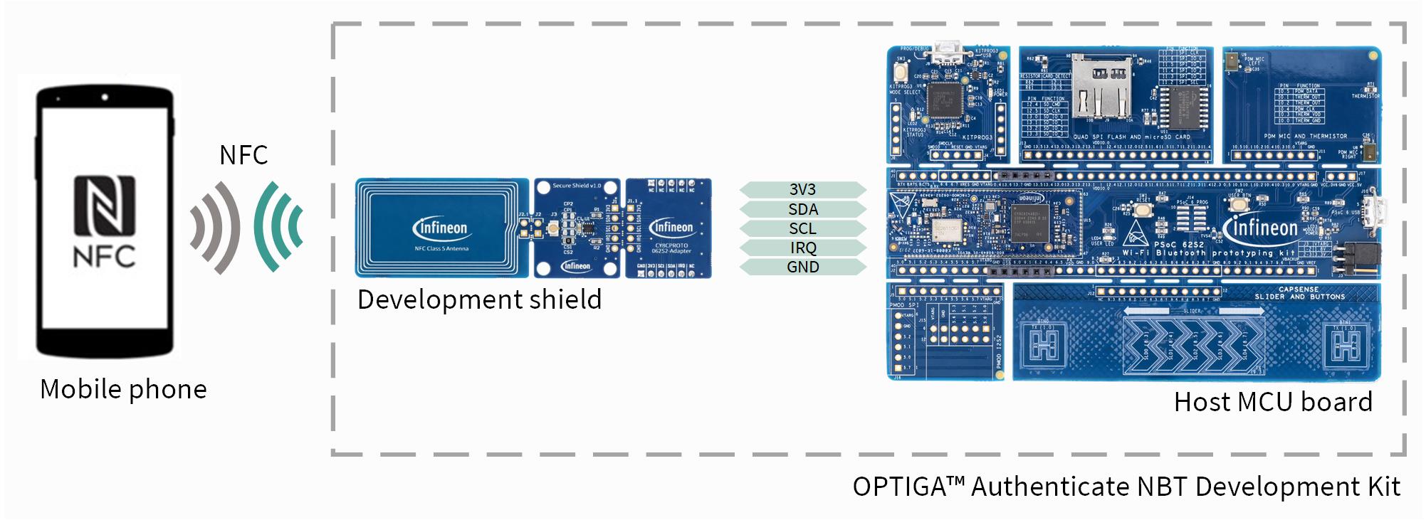
Fig. 87 Hardware components for operation.
Software
The involved software divides into the mobile phone app (Android or iOS), the application(s) running on the OPTIGA™ Authenticate NBT, and the embedded application (running on the host MCU PSOC™ board). The following figure shows an overview of the involved software components:
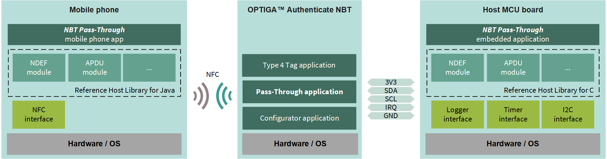
Fig. 88 Software architecture of the included applications for the operational use case.
The mobile phone and embedded applications are provided as source code via GitHub (see Software requirements). They are considered off-chip software, which means they can be modified and recompiled.
In contrast, the NBT applications are considered on-chip software, pre-flashed on the device and not alterable. The operational flow utilizes only the Pass-Through application of the OPTIGA™ Authenticate NBT’s on-chip applications. Refer to the extended datasheet for more information about the on-chip applications.
Operational flow
The example implementation of this use case involves the control of an LED via NFC. The application flow of writing and reading the LED status as well as design details can be found below.
In PT mode, the OPTIGA™ Authenticate NBT acts as a synchronous NFC to I2C bridge between the mobile phone and the host device which is connected via I2C to the OPTIGA™ Authenticate NBT. This means that the OPTIGA™ Authenticate NBT allows direct communication between the mobile phone and the host device by tunneling bi-directional communication between the NFC and I2C interfaces.
To perform a synchronous data transfer via PT, the mobile phone initiates an NFC communication, selects the proprietary demo application on the host system (that is not present on the OPTIGA™ Authenticate NBT itself), and then uses proprietary, application-specific commands to control the LED on the host.
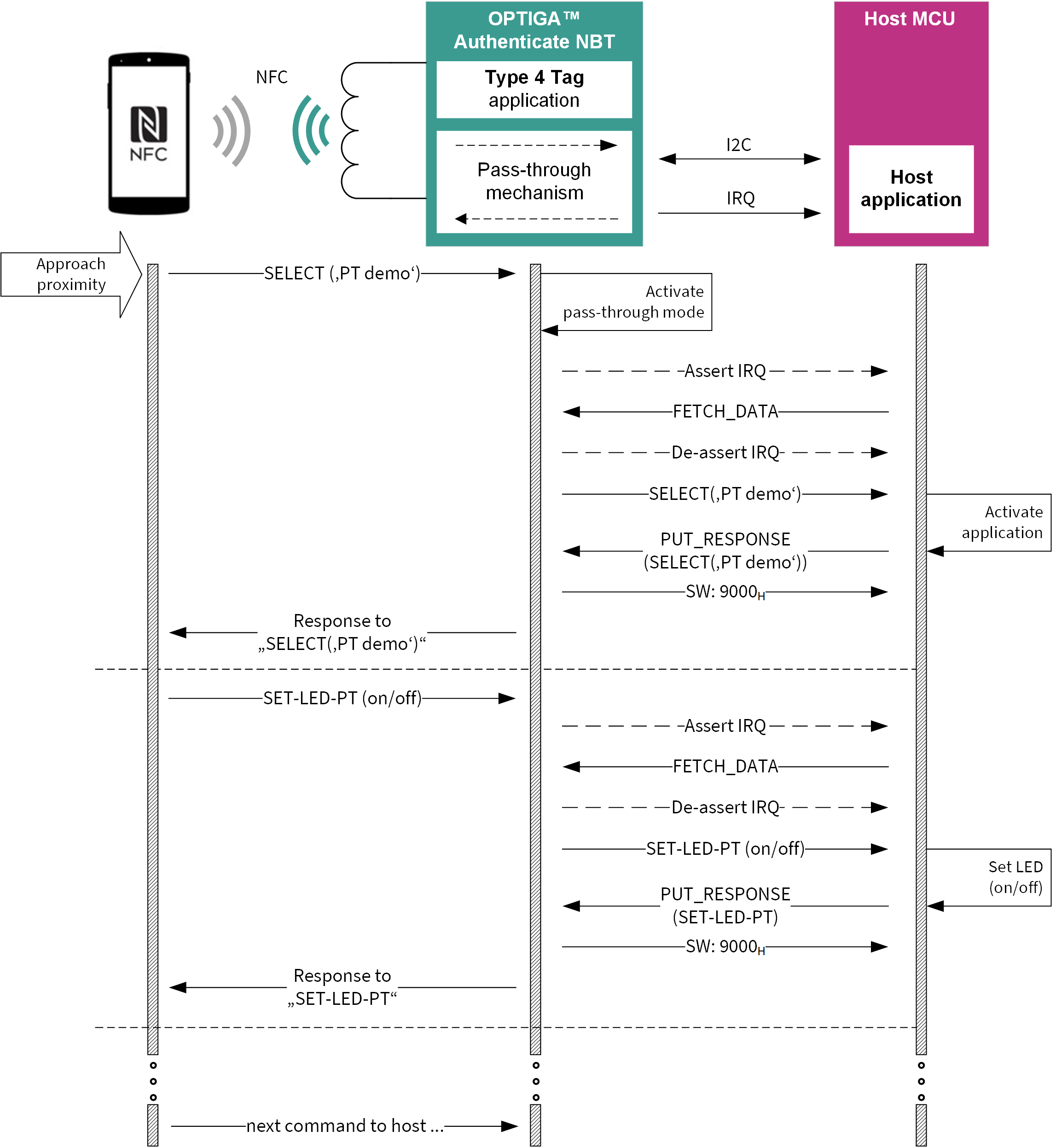
Fig. 89 Read/Write the state of the LED.
Design details
Describes the core design principles used for the implementation of the applications to demonstrate this use case. Additionally, cross-application definitions are stated here.
Data encoding
PT demo Application ID |
|
LED state = on |
|
LED state = off |
|
Custom PT commands
The OPTIGA™ Authenticate NBT automatically enters the pass-through mode, after a non-existing application is selected (SELECT command with a non-existing AID). In that mode, the MCU is notified and all upcoming APDU commands received by the OPTIGA™ Authenticate NBT via NFC are forwarded to the MCU (via I2C). The MCU implements the handling of these APDU commands and puts a response of that APDU to the NBT, which then returns that response via NFC.
In order to control the LED, a specific custom application has the be selected and a special APDU containing the desired led state has to be transferred.
The following table shows the supported APDUs of the host application.
Command |
Data |
Description |
|---|---|---|
SELECT (PT demo) |
|
Activates the PT host application |
SET-LED-PT |
|
Controls the host board’s LED |
IRQ handling
The IRQ line is used for two purposes:
To control the I2C communication between the OPTIGA™ Authenticate NBT and the host MCU.
Tpó signal to the host MCU that new NFC data has been received by the OPTIGA™ Authenticate NBT in pass-through mode.
Thus, the host MCU needs to distinguish between the two cases (IRQ signalling PT data available vs. I2C data transfer control). See the extended dataset for more information.
Pin mapping
Development shield |
MCU |
Function |
|---|---|---|
SDA |
P6.1 (CYBSP_I2C_SDA) |
I2C data |
SCL |
P6.0 (CYBSP_I2C_SCL) |
I2C clock |
IRQ |
P6.2 |
Interrupt |
3V3 |
VDD |
Power and pad supply (3V3) |
GND |
GND |
Common ground reference |