|
CAT2 Peripheral Driver Library
|
|
CAT2 Peripheral Driver Library
|
This driver configures and controls the SAR ADC subsystem block. More...
Modules | |
| Macros | |
| Functions | |
| Data Structures | |
| Enumerated Types | |
This driver configures and controls the SAR ADC subsystem block.
The functions and other declarations used in this driver are in cy_sar.h. You can include cy_pdl.h to get access to all functions and declarations in the PDL.
This SAR ADC subsystem is comprised of:
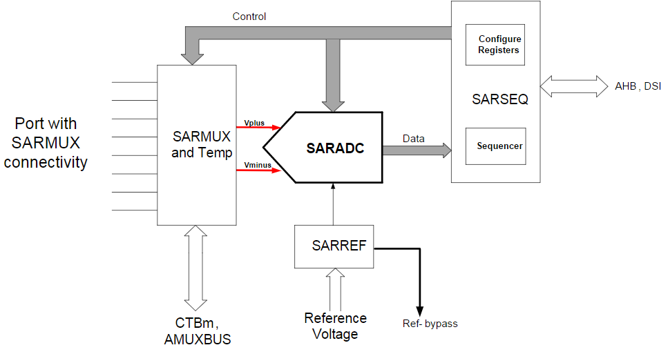
The high level features of the subsystem are:
As an example, following SAR configuration will be used:
The high level steps to use SAR driver are:
To configure the SAR subsystem, call Cy_SAR_Init. This function requires two pointers: a pointer to the SAR_Type structure for the base hardware register address and pointer to the configuration structure cy_stc_sar_config_t.
Configuration structure cy_stc_sar_config_t includes two substructures: cy_stc_sar_config_t::channelConfig and cy_stc_sar_config_t::routingConfig.
cy_stc_sar_channel_config_t is used to configure individual channels. Here is an example of SAR channels configuration for our use case:
cy_stc_sar_routing_config_t is used to define SARMUX configuration. Use one or more values from the SARMUX Switch Control Register Masks and "OR" them together. Firmware control can be changed at run-time by calling Cy_SAR_SetAnalogSwitch the desired switch states SARSEQ control can be changed at run-time by calling Cy_SAR_SetSwitchSarSeqCtrl.
Firmware control also can be changed at run-time by calling Cy_SAR_SetDiagSwitch the desired switch states SARSEQ control can be changed at run-time by calling Cy_SAR_SetDiagHwCtrl for the DIAGMUX/EXPMUX
In order to complete SAR configuration structure, all remaining fields of cy_stc_sar_config_t should be filled:
As mentioned in a previous step, to configure the SAR subsystem, call Cy_SAR_Init function with pointers to SAR_Type and cy_stc_sar_config_t structures. After initialization, call Cy_SAR_Enable to enable the hardware.
The SAR requires a clock. Assign a clock to the SAR using the pre-defined enum, PCLK_PASS_CLOCK_SAR, to identify the SAR subsystem. Set the clock divider value to achieve the desired clock rate. The SAR can support a maximum frequency of 18 MHz.
The SAR subsystem has the following modes for triggering a conversion:
| Mode | Description | Usage |
|---|---|---|
| Continuous | After completing a scan, the SARSEQ will immediately start the next scan. That is, the SARSEQ will always be BUSY. As a result all other triggers, firmware or hardware, are essentially ignored. | To enter this mode, call Cy_SAR_StartConvert with CY_SAR_START_CONVERT_CONTINUOUS. To stop continuous conversions, call Cy_SAR_StopConvert. |
| Firmware single shot | A single conversion of all enabled channels is triggered with a function call to Cy_SAR_StartConvert with CY_SAR_START_CONVERT_SINGLE_SHOT. | Firmware triggering is always available by calling Cy_SAR_StartConvert with CY_SAR_START_CONVERT_SINGLE_SHOT. To allow only firmware triggering, or disable hardware triggering, set up the cy_stc_sar_config_t::trigMode field of config structure with CY_SAR_TRIGGER_MODE_FW_ONLY. |
| Hardware edge sensitive | A single conversion of all enabled channels is triggered on the rising edge of the hardware trigger signal. | To enable this mode, set up the cy_stc_sar_config_t::trigMode field of config structure with CY_SAR_TRIGGER_MODE_FW_AND_HWEDGE. |
| Hardware level sensitive | Conversions are triggered continuously when the hardware trigger signal is high. | To enable this mode, set up the cy_stc_sar_config_t::trigMode field of config structure with CY_SAR_TRIGGER_MODE_FW_AND_HWLEVEL. |
If the trigger occurs during a scan, a CY_SAR_INTR_FW_COLLISION interrupt occurs and the trigger is delayed until the end of the scan.
The trigger mode can be changed during run time with Cy_SAR_SetConvertMode.
For the hardware trigger modes, use the TrigMux (Trigger Multiplexer) driver to route an internal or external signal to the SAR trigger input. When making the required Cy_TrigMux_Connect calls, use the pre-defined enum, TRIG6_OUT_PASS_TR_SAR_IN, for the SAR trigger input.
The SAR can generate interrupts on these events:
The SAR interrupt to the NVIC is raised any time the intersection (logic and) of the interrupt flags and the corresponding interrupt masks are non-zero.
Implement an interrupt routine and assign it to the SAR interrupt. Use the pre-defined enum, pass_interrupt_sar_IRQn, as the interrupt source for the SAR.
The following code snippet demonstrates how to implement a routine to handle the interrupt. The routine gets called when any one of the SAR interrupts are triggered. When servicing an interrupt, the user must clear the interrupt so that subsequent interrupts can be handled.
The following code snippet demonstrates how to configure and enable the interrupt.
Alternately, instead of handling the interrupts, the Cy_SAR_IsEndConversion function allows for firmware polling of the end of conversion status.
Retrieve the ADC result by calling Cy_SAR_GetResult16 with the desired channel. To convert the result to a voltage, pass the ADC result to Cy_SAR_CountsTo_Volts, Cy_SAR_CountsTo_mVolts, or Cy_SAR_CountsTo_uVolts. To customize the counts-to-volts conversion process, use Cy_SAR_SetChannelOffset and Cy_SAR_SetChannelGain functions.
The scan rate is dependent on the following:
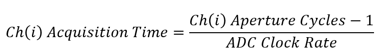
The acquisition time of a channel is based on which of the four global aperture times are selected for that channel. The selection is done during initialization per channel with cy_stc_sar_channel_config_t. The four global aperture times are also set during initialization with from cy_stc_sar_config_t::sampleTime0 through cy_stc_sar_config_t::sampleTime3. Note that these global aperture times are in SAR clock cycles and the acquisition time is 1 less than that value in the register.
The sample time for a channel is the time required to acquire the analog signal and convert it to a digital code.
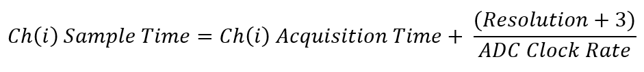
The SAR ADC is a 12-bit converter so Resolution = 12.
Channels using one of the sequential averaging modes: accumulating or fixed (see cy_stc_sar_config_t::avgShift) are sampled multiple times per scan. The number of samples averaged are set during initialization using cy_stc_sar_config_t::avgCnt. Channels that are not averaged are only sampled once per scan.
The total scan time is the sum of each channel's sample time multiplied by the samples per scan.
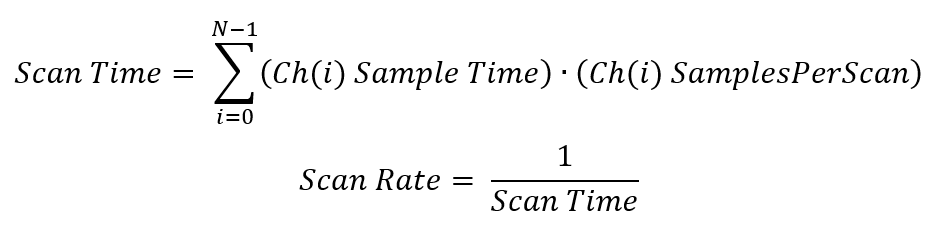
where N is the total number of channels in the scan.
The SARMUX is an analog programmable multiplexer. Its switches can be controlled by the SARSEQ or firmware. and the inputs can come from:
The following figure shows the SARMUX switches. See the device datasheet for the exact location of SARMUX pins.
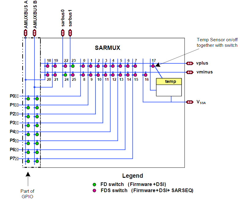
When using the SARSEQ, the following configurations must be performed:
While firmware can control every switch in the SARMUX, not every switch can be controlled by the SARSEQ (green switches in the above figure). Additionally, switches outside of the SARMUX such as the AMUXBUSA/B switches or CTB switches will require separate function calls (see GPIO and CTB drivers). The SARSEQ can control three switches in the CTB driver. These switches need to be enabled for SARSEQ control if the CTB outputs are used as the SARMUX inputs.
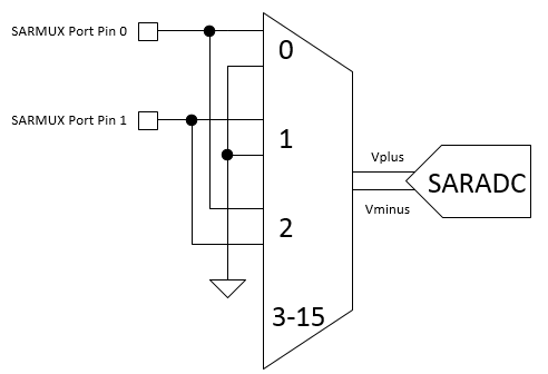
The following figure and code snippet show how two GPIOs on the SARMUX dedicated port are connected to the SARADC as separate single-ended channels and as a differential-pair channel.
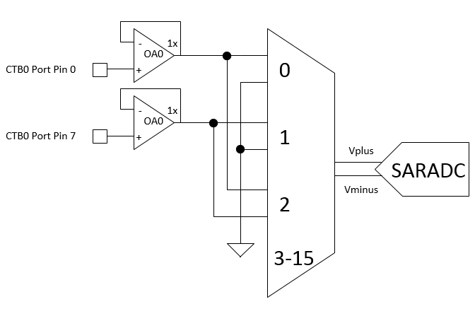
The following figure and code snippet show how the two opamp outputs from the CTB are connected to the SARADC as separate single-ended channels and as a differential-pair channel. Note that separate function calls are needed to configure and enable the opamps, perform required analog routing, and enable SARSEQ control of the switches contained in the CTB.
Use Input from SARMUX port code snippet for reference.
Then use Cy_SAR_Init and results retrieval as usual. For more information about CTB see CTB (Continuous Time Block).
The following figure and code snippet show how two GPIOs on any port through the AMUXBUSA and AMUXBUSB are connected to the SARADC as separate single-ended channels and as a differential-pair channel. Note that separate function calls are needed to route the device pins to the SARMUX. The AMUXBUSes are separated into multiple segments and these segments are connected/disconnected using the AMUX_SPLIT_CTL registers in the HSIOM.
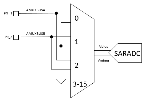
Use Input from SARMUX port code snippet for reference.
To connect SARMUX to any other non-dedicated port, you may need to close additional HSIOM switches to route signals through AMUXBUS. For more detail, see the device TRM, AMUX splitting.
The following code snippet is an alternative pin configuration. To connect Port 1 to AMUXBUS, close the left and right switches of AMUX_SPLIT_CTL[1] and AMUX_SPLIT_CTL[6].
The DieTemp sensor scanning typically is being done by the injection channel:
Then the regular initialization is going on:
Then during the ADC working the injection channel is being activated:
Then the retrieved injection channel result can be transformed into the temperature value:
This SAR driver provides a callback function to handle power mode transitions. The Cy_SAR_DeepSleepCallback function ensures that SAR conversions are stopped before Deep Sleep entry. Upon wakeup, the callback enables the hardware and continuous conversions, if previously enabled.
To trigger the callback execution, the callback must be registered before calling Cy_SysPm_CpuEnterDeepSleep. Refer to SysPm (System Power Management) driver for more information about power mode transitions and callback registration.
Recall that during configuration the SARMUX can be configured to remain enabled in Deep Sleep mode by the cy_stc_sar_config_t::sarMuxDsEn setting. All other blocks (SARADC, REFBUF, and SARSEQ) do not support Deep Sleep mode operation.
For more information on the SAR ADC subsystem, refer to the technical reference manual (TRM).
| Version | Changes | Reason for Change |
|---|---|---|
| 2.90 | Added Dynamic IMO only for new 4100S Plus devices. | New feature support. |
| 2.80 | Fixed an issue related to using EXPMUX. | Bug fixing. |
| 2.70 | Added the Cy_SAR_SetAveragingMode function. | API improvement |
| 2.60 | Added support of PSOC 4100T Plus device family. | New device support. |
| Re-defined settings of the SAR_DFT_CTRL_DCEN bit in the Cy_SAR_Init() and Cy_SAR_SetVref() functions. | Bug fixing. | |
| Temperature ranges are updated in the Cy_SAR_CountsTo_degreeC() function. | Bug fixing. | |
| The cy_stc_sar_config_t::sampleTime0 description is updated. | Documentation improvement. | |
| 2.50 | Added the Cy_SAR_CountsTo_degreeC function | API improvement |
| The configuration restoring during DeepSleep cycle is updated in the Cy_SAR_DeepSleepCallback function | Bug fix | |
| 2.40 | Added support for a new version of SAR. Added support for PSOC4 HVMS/PA platform. Updated APIs to incorporate PSOC4 HVMS/PA platform configuration. Documentation enhancement. | New device support. |
| 2.30 | The Cy_SAR_DeepSleepCallback parameter type is changed to match with the cy_stc_syspm_callback_t::callback type | Eliminate compiler warnings |
| The Cy_SAR_IsEndConversion timeout is corrected | Fixed incorrect timeout value and related documentation | |
| 2.20 | The Cy_SAR_CountsTo_uVolts is updated to avoid 64-bit math | Memory consumption reduction |
| Update the paths to the code snippets. | PDL structure update. | |
| 2.10 | Added the cy_stc_sar_channel_config_t::rangeIntrEn and cy_stc_sar_channel_config_t::satIntrEn settings | Bug fixing |
| Fixed the Cy_SAR_SetConvertMode function | Bug fixing | |
| Updated the Cy_SAR_CountsTo_uVolts, Cy_SAR_CountsTo_mVolts and Cy_SAR_CountsTo_Volts functions so that they now support sub-resolutions | Bug fixing | |
| 2.0 | Added the Cy_SAR_CountsTo_degreeC function | Die temperature measurement support |
| Added the Cy_SAR_EnableChannels and Cy_SAR_DisableChannels functions | API enhancement | |
| Added code snippets how to interconnect with CTB (Continuous Time Block) | CTB (Continuous Time Block) support | |
| The type of cy_stc_sar_channel_config_t::sampleTimeSel is changed from uint32_t to cy_en_sar_channel_sampletime_t | Improved the API error proofness | |
| 1.0.1 | Minor documentation updates. | Documentation enhancement |
| 1.0 | Initial version |