|
CAT2 Peripheral Driver Library
|
|
CAT2 Peripheral Driver Library
|
This driver provides API functions to configure and use the analog CTB. More...
Modules | |
| Macros | |
| Functions | |
| Data Structures | |
| Enumerated Types | |
| Enumerated Types | |
This driver provides API functions to configure and use the analog CTB.
The functions and other declarations used in this driver are in cy_ctb.h. You can include cy_pdl.h to get access to all functions and declarations in the PDL.
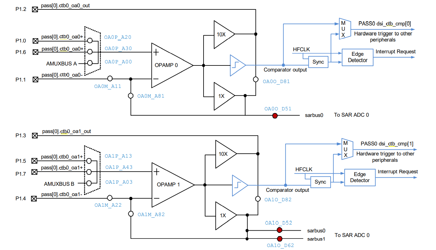
The CTB comprises two identical operational amplifiers (opamps) and a switch routing matrix. The high-level features are:
Each opamp, marked OA0 and OA1, has one input and three output stages, all of which share the common input stage. The only one output stage can be selected at a time.
The output stage can operate as a low-drive strength opamp for internal connections (1X), a high-drive strength opamp for driving a device pin (10X), or a comparator.
Using the switching matrix, the opamp inputs and outputs can be connected to dedicated general-purpose I/Os or other internal analog blocks. See the device datasheet for the dedicated CTB port.
Before enabling the CTB, set up any external components (such as resistors) needed for the design.
To configure the entire hardware CTB block, call Cy_CTB_Init. Alternatively, to configure only one opamp, call Cy_CTB_OpampInit. The base address of the CTB hardware can be found in the device specific header file.
After initialization, call Cy_CTB_Enable to enable the hardware.
The CTB has internal switches to support flexible input and output routing. If these switches have not been configured during initialization, call Cy_CTB_SetAnalogSwitch to make the input and output connections. See the architecture TRM for more details.
As shown in the CTB switch diagram, the external (10x) output of OA0 and OA1 have dedicated connections. If different output connections are required, the AMUXBUX A/B switches can be used.
Each opamp can be configured as a comparator. Note that when used as a comparator, the hardware shuts down the 1X and 10X output drivers. Specific to Comparator mode, there is an optional 10 mV input hysteresis and configurable edge detection interrupt handling.
The comparator output can be routed to a pin or other component using HSIOM or trigger muxes.
The comparator output is connected to an edge detector block used to detect the edge (rising, falling, both, or disabled) for interrupt generation.
The following code snippet demonstrates how to implement a routine to handle the interrupt. The routine gets called when any comparator on the device generates an interrupt.
The following code snippet demonstrates how to configure and enable the interrupt.
The input range of the opamp can be rail-to-rail if the charge pump is enabled. See the device datasheet for more details.
The CTB relies on other blocks to function properly. The dependencies are documented here.
Each opamp of the CTB has a charge pump that when enabled increases the input range to the supply rails. Call the Cy_PASS_SetPumpClkSource function to set the clock source for all CTBs and SAR ADC. This clock can come from one of three sources:
The dedicated clock from the SRSS
Call the following functions to configure the pump clock from the SRSS:
The high frequency clock
The CTB uses reference current generator from the Deep-Sleep Amplifier Bias (DSAB) block.
If the CTB is configured to operate in Deep Sleep mode, the appropriate reference current generator from the DSAB block must be enabled in Deep Sleep.
Refer to technical reference manual (TRM) and the device datasheet.
| Version | Changes | Reason for Change |
|---|---|---|
| 1.10 | Added Cy_PASS_ClkPumpSetSource() to set source of pump clock for PASS block | Defect fixes |
| 1.0.1 | Update the paths to the code snippets. | PDL structure update. |
| 1.0 | Initial version |