 |
PSoC 6 Peripheral Driver Library
|
|
PSoC 6 Peripheral Driver Library
|
This driver configures and controls the SAR ADC subsystem block.
The functions and other declarations used in this driver are in cy_sar.h. You can include cy_pdl.h to get access to all functions and declarations in the PDL.
This SAR ADC subsystem is comprised of:
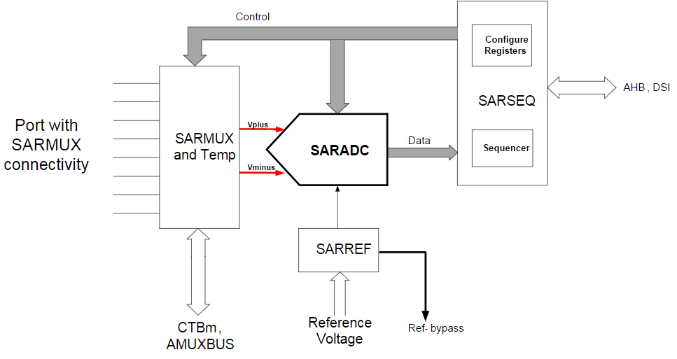
The high level features of the subsystem are:
The high level steps to use this driver are:
To configure the SAR subsystem, call Cy_SAR_Init. Pass in a pointer to the SAR_Type structure for the base hardware register address and pass in the configuration structure, cy_stc_sar_config_t.
After initialization, call Cy_SAR_Enable to enable the hardware.
Here is guidance on how to set the data fields of the configuration structure:
This field specifies configurations that apply to all channels such as the Vref source or the negative terminal selection for all single-ended channels. Select a value from each of the following enums that begin with "cy_en_sar_ctrl_" and "OR" them together.
This field configures sampling details that apply to all channels. Select a value from each of the following enums that begin with "cy_en_sar_sample_" and "OR" them together.
This field configures the value for sample times 0 and 1 in ADC clock cycles.
The SAR has four programmable 10-bit aperture times that are configured using two data fields, uint32_t sampleTime01 and uint32_t sampleTime23. Ten bits allow for a range of 0 to 1023 cycles, however 0 and 1 are invalid. The minimum aperture time is 167 ns. With an 18 MHz ADC clock, this is equal to 3 cycles or a value of 4 in this field. The actual aperture time is one cycle less than the value stored in this field.
Use the shifts defined in cy_en_sar_sample_time_shift_t.
This field configures the value for sample times 2 and 3 in ADC clock cycles. Use the shifts defined in cy_en_sar_sample_time_shift_t.
This field configures the upper and lower thresholds for the range interrupt. These thresholds apply on a global level for all channels with range detection enabled.
The SARSEQ supports range detection to allow for automatic detection of sample values compared to two programmable thresholds without CPU involvement. Range detection is done after averaging, alignment, and sign extension (if applicable). In other words the threshold values need to have the same data format as the result data. The values are interpreted as signed or unsigned according to each channel's configuration.
Use the shifts defined in cy_en_sar_range_thres_shift_t.
The Cy_SAR_SetLowLimit and Cy_SAR_SetHighLimit provide run-time configurability of these thresholds.
This field configures the condition (below, inside, outside, or above) that will trigger the range interrupt. Select a value from the cy_en_sar_range_detect_condition_t enum.
This field configures which channels will be scanned. Each bit corresponds to a channel. Bit 0 enables channel 0, bit 1 enables channel 1, bit 2 enables channel 2, and so on.
Each channel has its own channel configuration register. The channel configuration specifies which pin/signal is connected to that channel and how the channel is sampled.
Select a value from each of the following enums that begin with "cy_en_sar_chan_config_" and "OR" them together.
Some important considerations are:
If the SARSEQ is disabled (cy_en_sar_ctrl_sarseq_routing_switches_t) or it is not controlling any switches (uint32_t muxSwitchSqCtrl = 0), the port and pin addresses are ignored. This is possible when there is only one channel to scan.
This field configures which interrupt events (end of scan, overflow, or firmware collision) will be serviced by the firmware.
Select one or more values from the cy_en_sar_intr_mask_t enum and "OR" them together.
This field configures which channels will cause a saturation interrupt.
The SARSEQ has a saturation detect that is always applied to every conversion. This feature detects whether a channel's sample value is equal to the minimum or maximum values. This allows the firmware to take action, for example, discard the result, when the SARADC saturates. The sample value is tested right after conversion, that is, before averaging. This means that it can happen that the interrupt is set while the averaged result in the data register is not equal to the minimum or maximum.
Each bit corresponds to a channel. A value of 0 disables saturation detection for all channels.
This field configures which channels will cause a range detection interrupt. Each bit corresponds to a channel. A value of 0 disables range detection for all channels.
This field is the firmware control of the SARMUX switches.
Use one or more values from the cy_en_sar_mux_switch_fw_ctrl_t enum and "OR" them together. If the SARSEQ is enabled, the SARMUX switches that will be used must also be closed using this firmware control.
Firmware control can be changed at run-time by calling Cy_SAR_SetAnalogSwitch with CY_SAR_MUX_SWITCH0 and the desired switch states.
This field enables or disables SARSEQ control of the SARMUX switches. To disable control of all switches, set this field to 0. To disable the SARSEQ all together, use CY_SAR_SARSEQ_SWITCH_DISABLE when configuring the uint32_t ctrl register.
Use one or more values from the cy_en_sar_mux_switch_sq_ctrl_t enum and "OR" them together.
SARSEQ control can be changed at run-time by calling Cy_SAR_SetSwitchSarSeqCtrl.
If true, the uint32_t muxSwitch and uint32_t muxSwitchSqCtrl fields will be used. If false, the fields will be ignored.
This field sets the value of the reference voltage in millivolts used. This value is used for converting counts to volts in the Cy_SAR_CountsTo_Volts, Cy_SAR_CountsTo_mVolts, and Cy_SAR_CountsTo_uVolts functions.
The SAR subsystem has the following modes for triggering a conversion:
| Mode | Description | Usage |
|---|---|---|
| Continuous | After completing a scan, the SARSEQ will immediately start the next scan. That is, the SARSEQ will always be BUSY. As a result all other triggers, firmware or hardware, are essentially ignored. | To enter this mode, call Cy_SAR_StartConvert with CY_SAR_START_CONVERT_CONTINUOUS. To stop continuous conversions, call Cy_SAR_StopConvert. |
| Firmware single shot | A single conversion of all enabled channels is triggered with a function call to Cy_SAR_StartConvert with CY_SAR_START_CONVERT_SINGLE_SHOT. | Firmware triggering is always available by calling Cy_SAR_StartConvert with CY_SAR_START_CONVERT_SINGLE_SHOT. To allow only firmware triggering, or disable hardware triggering, set up the cy_stc_sar_config_t config structure with CY_SAR_TRIGGER_MODE_FW_ONLY. |
| Hardware edge sensitive | A single conversion of all enabled channels is triggered on the rising edge of the hardware trigger signal. | To enable this mode, set up the cy_stc_sar_config_t config structure with CY_SAR_TRIGGER_MODE_FW_AND_HWEDGE. |
| Hardware level sensitive | Conversions are triggered continuously when the hardware trigger signal is high. | To enable this mode, set up the cy_stc_sar_config_t config structure with CY_SAR_TRIGGER_MODE_FW_AND_HWLEVEL. |
The trigger mode can be changed during run time with Cy_SAR_SetConvertMode.
For the hardware trigger modes, use the TrigMux (Trigger Multiplexer) driver to route an internal or external signal to the SAR trigger input. When making the required Cy_TrigMux_Connect calls, use the pre-defined enum, TRIG6_OUT_PASS_TR_SAR_IN, for the SAR trigger input.
The SAR can generate interrupts on these events:
The SAR interrupt to the NVIC is raised any time the intersection (logic and) of the interrupt flags and the corresponding interrupt masks are non-zero.
Implement an interrupt routine and assign it to the SAR interrupt. Use the pre-defined enum, pass_interrupt_sar_IRQn, as the interrupt source for the SAR.
The following code snippet demonstrates how to implement a routine to handle the interrupt. The routine gets called when any one of the SAR interrupts are triggered. When servicing an interrupt, the user must clear the interrupt so that subsequent interrupts can be handled.
The following code snippet demonstrates how to configure and enable the interrupt.
Alternately, instead of handling the interrupts, the Cy_SAR_IsEndConversion function allows for firmware polling of the end of conversion status.
Retrieve the ADC result by calling Cy_SAR_GetResult16 with the desired channel. To convert the result to a voltage, pass the ADC result to Cy_SAR_CountsTo_Volts, Cy_SAR_CountsTo_mVolts, or Cy_SAR_CountsTo_uVolts.
The SAR requires a clock. Assign a clock to the SAR using the pre-defined enum, PCLK_PASS_CLOCK_SAR, to identify the SAR subsystem. Set the clock divider value to achieve the desired clock rate. The SAR can support a maximum frequency of 18 MHz.
The scan rate is dependent on the following:
The acquisition time of a channel is based on which of the four global aperture times are selected for that channel. The selection is done during initialization per channel with uint32_t chanConfig[16]. The four global aperture times are also set during initialization with uint32_t sampleTime01 and uint32_t sampleTime23. Note that these global aperture times are in SAR clock cycles and the acquisition time is 1 less than that value in the register.
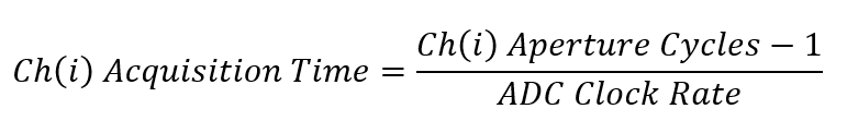
The sample time for a channel is the time required to acquire the analog signal and convert it to a digital code.
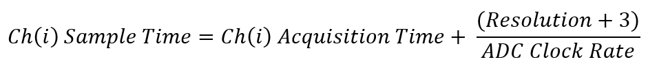
The SAR ADC is a 12-bit converter so Resolution = 12.
Channels using one of the sequential averaging modes (CY_SAR_AVG_MODE_SEQUENTIAL_ACCUM or CY_SAR_AVG_MODE_SEQUENTIAL_FIXED) are sampled multiple times per scan. The number of samples averaged are set during initialization with uint32_t sampleCtrl using one of the values from cy_en_sar_sample_ctrl_avg_cnt_t. Channels that are not averaged or use the CY_SAR_AVG_MODE_INTERLEAVED mode are only sampled once per scan.
The total scan time is the sum of each channel's sample time multiplied by the samples per scan.
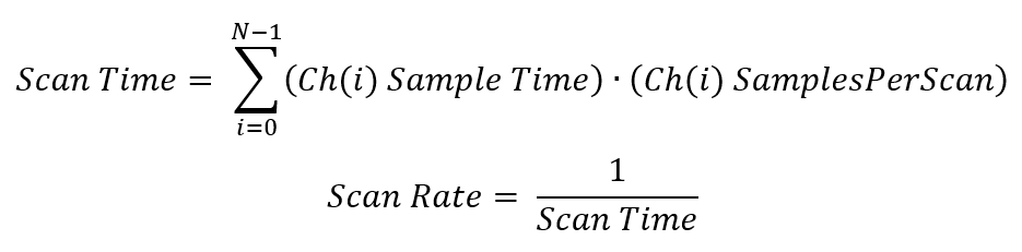
where N is the total number of channels in the scan.
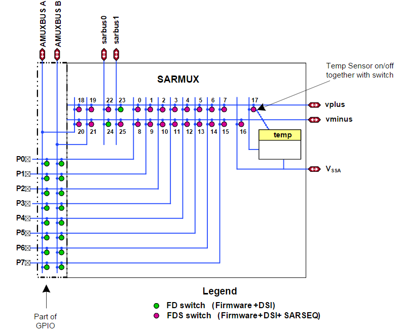
The SARMUX is an analog programmable multiplexer. Its switches can be controlled by the SARSEQ or firmware. and the inputs can come from:
The following figure shows the SARMUX switches. See the device datasheet for the exact location of SARMUX pins.
When using the SARSEQ, the following configurations must be performed:
While firmware can control every switch in the SARMUX, not every switch can be controlled by the SARSEQ (green switches in the above figure). Additionally, switches outside of the SARMUX such as the AMUXBUSA/B switches or CTB switches will require separate function calls (see GPIO and CTB drivers). The SARSEQ can control three switches in the CTB driver (see Cy_CTB_EnableSarSeqCtrl). These switches need to be enabled for SARSEQ control if the CTB outputs are used as the SARMUX inputs.
The following table shows the required POS_PORT_ADDR and POS_PIN_ADDR settings for different input connections.
| Input Connection Selection | POS_PORT_ADDR | POS_PIN_ADDR |
|---|---|---|
| SARMUX dedicated port | CY_SAR_POS_PORT_ADDR_SARMUX | CY_SAR_CHAN_POS_PIN_ADDR_0 through CY_SAR_CHAN_POS_PIN_ADDR_7 |
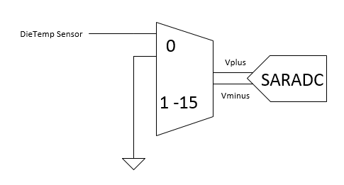
| DieTemp sensor | CY_SAR_POS_PORT_ADDR_SARMUX_VIRT | CY_SAR_CHAN_POS_PIN_ADDR_0 |
| AMUXBUSA | CY_SAR_POS_PORT_ADDR_SARMUX_VIRT | CY_SAR_CHAN_POS_PIN_ADDR_2 |
| AMUXBUSB | CY_SAR_POS_PORT_ADDR_SARMUX_VIRT | CY_SAR_CHAN_POS_PIN_ADDR_3 |
| CTB0 Opamp0 1x output | CY_SAR_POS_PORT_ADDR_CTB0 | CY_SAR_CHAN_POS_PIN_ADDR_2 |
| CTB0 Opamp1 1x output | CY_SAR_POS_PORT_ADDR_CTB0 | CY_SAR_CHAN_POS_PIN_ADDR_3 |
When using the DieTemp sensor, always use single-ended mode. The temperature sensor can be routed to Vplus using the CY_SAR_MUX_FW_TEMP_VPLUS switch. Connecting this switch will also enable the sensor. Set the acquisition time to be at least 1 us to meet the settling time of the temperature sensor.
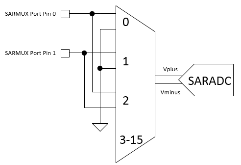
The following figure and code snippet show how two GPIOs on the SARMUX dedicated port are connected to the SARADC as separate single-ended channels and as a differential-pair channel.
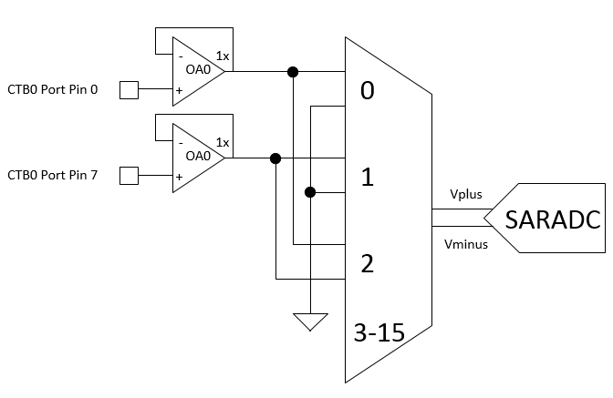
The following figure and code snippet show how the two opamp outputs from the CTB are connected to the SARADC as separate single-ended channels and as a differential-pair channel. Note that separate function calls are needed to configure and enable the opamps, perform required analog routing, and enable SARSEQ control of the switches contained in the CTB.
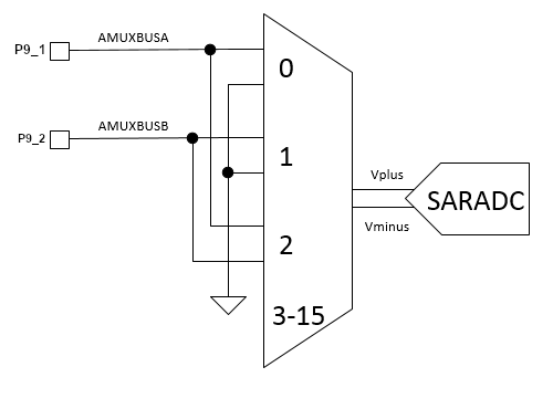
The following figure and code snippet show how two GPIOs on any port through the AMUXBUSA and AMUXBUSB are connected to the SARADC as separate single-ended channels and as a differential-pair channel. Note that separate function calls are needed to route the device pins to the SARMUX. The AMUXBUSes are separated into multiple segments and these segments are connected/disconnected using the AMUX_SPLIT_CTL registers in the HSIOM.
To connect SARMUX to any other non-dedicated port, you may need to close additional HSIOM switches to route signals through AMUXBUS. For more detail, see the device TRM, AMUX splitting.
The following code snippet is an alternative pin configuration. To connect Port 1 to AMUXBUS, close the left and right switches of AMUX_SPLIT_CTL[1] and AMUX_SPLIT_CTL[6].
This SAR driver provides a callback function to handle power mode transitions. The Cy_SAR_DeepSleepCallback function ensures that SAR conversions are stopped before Deep Sleep entry. Upon wakeup, the callback enables the hardware and continuous conversions, if previously enabled.
To trigger the callback execution, the callback must be registered before calling Cy_SysPm_CpuEnterDeepSleep. Refer to SysPm (System Power Management) driver for more information about power mode transitions and callback registration.
Recall that during configuration of the ctrl field, the SARMUX can be configured to remain enabled in Deep Sleep mode. All other blocks (SARADC, REFBUF, and SARSEQ) do not support Deep Sleep mode operation.
For more information on the SAR ADC subsystem, refer to the technical reference manual (TRM).
This driver has the following specific deviations:
| MISRA Rule | Rule Class (Required/Advisory) | Rule Description | Description of Deviation(s) |
|---|---|---|---|
| 11.4 | Advisory | A cast should not be performed between a pointer to object type and a different pointer to object type. | The cy_syspm driver defines the pointer to void in the cy_stc_syspm_callback_params_t::base field. This SAR driver implements a Deep Sleep callback conforming to the cy_syspm driver requirements. When the callback is called, the base should point to the SAR_Type register address. |
| Version | Changes | Reason for Change |
|---|---|---|
| 1.20.3 | Minor documentation updates. | Documentation enhancement. |
| 1.20.2 | Code snippets update. | PDL infrastructure update, documentation enhancement. |
| 1.20.1 | Code snippets update. | PDL infrastructure update, documentation enhancement. |
| 1.20 | Flattened the organization of the driver source code into the single source directory and the single include directory. | Driver library directory-structure simplification. |
| Added register access layer. Use register access macros instead of direct register access using dereferenced pointers. | Makes register access device-independent, so that the PDL does not need to be recompiled for each supported part number. | |
| 1.10 | Added workaround for parts with out of range CAP_TRIM in Init API. | Correct CAP_TRIM is necessary achieving specified SAR ADC linearity |
| Turn off the entire hardware block only if the SARMUX is not enabled for Deep Sleep operation. | Improvement of the Cy_SAR_DeepSleep flow | |
| Updated "Low Power Support" section to describe registering the Deep Sleep callback. Added parenthesis around logical AND operation in Sleep API. | Documentation update and clarification | |
| 1.0 | Initial version |
API Reference | |
| Macros | |
| Functions | |
| Global Variables | |
| Data Structures | |
| Enumerated Types | |