 |
PSoC 6 Peripheral Driver Library
|
|
PSoC 6 Peripheral Driver Library
|
This driver provides API functions to configure and use the analog CTB.
The functions and other declarations used in this driver are in cy_ctb.h. You can include cy_pdl.h to get access to all functions and declarations in the PDL.
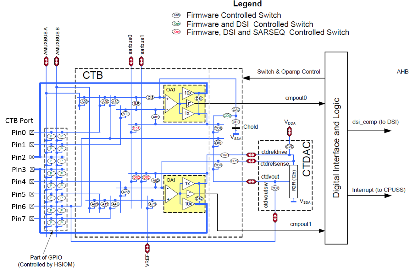
The CTB comprises two identical opamps, a switch routing matrix, and a sample and hold (SH) circuit. The high level features are:
Each opamp, marked OA0 and OA1, has one input and three output stages, all of which share the common input stage. Note that only one output stage can be selected at a time. The output stage can operate as a low-drive strength opamp for internal connections (1X), a high-drive strength opamp for driving a device pin (10X), or a comparator.
Using the switching matrix, the opamp inputs and outputs can be connected to dedicated general-purpose I/Os or other internal analog blocks. See the device datasheet for the dedicated CTB port.
Before enabling the CTB, set up any external components (such as resistors) that are needed for the design. To configure the entire hardware block, call Cy_CTB_Init. The base address of the CTB hardware can be found in the device specific header file. Alternatively, to configure only one opamp without any routing, call Cy_CTB_OpampInit. The driver also provides a Cy_CTB_FastInit function for fast and easy initialization of the CTB based on commonly used configurations. They are pre-defined in the driver as:
Opamp0
Opamp1
After initialization, call Cy_CTB_Enable to enable the hardware.
The CTB has internal switches to support flexible input and output routing. If these switches have not been configured during initialization, call Cy_CTB_SetAnalogSwitch to make the input and output connections.
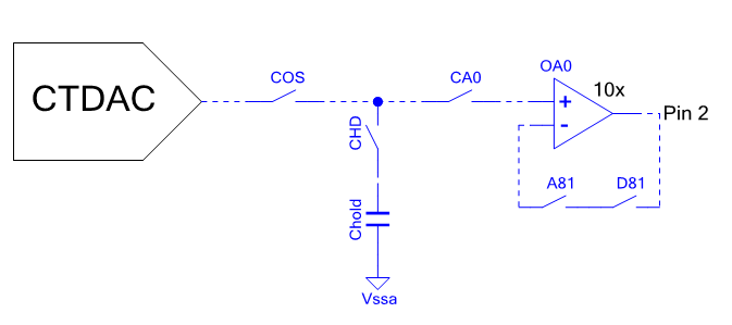
As shown in the CTB switch diagram, the 10x output of OA0 and OA1 have dedicated connections to Pin 2 and Pin 3, respectively, of the CTB port. If different output connections are required, the other CTB switches and/or AMUXBUX A/B switches can be used.
Each opamp can be configured as a comparator. Note that when used as a comparator, the hardware shuts down the 1X and 10X output drivers. Specific to the comparator mode, there is an optional 10 mV input hysteresis and configurable edge detection interrupt handling.
The comparator output can be routed to a pin or other components using HSIOM or trigger muxes.
The comparator output is connected to an edge detector block, which is used to detect the edge (rising, falling, both, or disabled) for interrupt generation.
The following code snippet demonstrates how to implement a routine to handle the interrupt. The routine gets called when any comparator on the device generates an interrupt.
The following code snippet demonstrates how to configure and enable the interrupt.
The input range of the opamp can be rail-to-rail if the charge pump is enabled. Without the charge pump, the input range is 0 V to VDDA - 1.5 V. The output range of the opamp is typically 0.2 V to VDDA - 0.2 V and will depend on the load. See the device datasheet for more detail.
| Charge Pump | Input Range | Output Range |
|---|---|---|
| Enabled | 0 V to VDDA | 0.2 V to VDDA - 0.2 V |
| Disabled | 0 V to VDDA - 1.5 V | 0.2 V to VDDA - 0.2 V |
The CTB has a sample and hold (SH) circuit at the non-inverting input of Opamp0. The circuit includes a hold capacitor, Chold, with a firmware controlled switch, CHD. Sampling and holding the source voltage is performed by closing and opening appropriate switches in the CTB using firmware. If the SH circuit is used for the CTDAC, the Cy_CTB_DACSampleAndHold function should be called.
The CTB relies on other blocks to function properly. The dependencies are documented here.
Each opamp of the CTB has a charge pump that when enabled increases the input range to the supply rails. When disabled, the opamp input range is 0 - VDDA - 1.5 V. When enabled, the pump requires a clock. Call the Cy_CTB_SetClkPumpSource function in the SysAnalog (System Analog Reference Block) driver to set the clock source for all CTBs. This clock can come from one of two sources:
A dedicated clock divider from one of the CLK_PATH in the SRSS
Call the following functions to configure the pump clock from the SRSS:
One of the Peri Clock dividers
Call the following functions to configure a Peri Clock divider as the pump clock:
When the charge pump is enabled, the clock frequency should be set as follows:
| Opamp Power Level | Pump Clock Freq |
|---|---|
| Low or Medium | 8 - 24 MHz |
| High | 24 MHz |
The High power level of the opamp requires a 24 MHz pump clock. In Deep Sleep mode, all high frequency clocks are disabled and the charge pump will be disabled.
The CTB uses two reference current generators, IPTAT and IZTAT, from the AREF block (see SysAnalog (System Analog Reference Block) driver). The IPTAT current is used to trim the slope of the opamp offset across temperature. The AREF must be initialized and enabled for the CTB to function properly.
If the CTB is configured to operate in Deep Sleep mode, the appropriate reference current generators from the AREF block must be enabled in Deep Sleep. When waking up from Deep Sleep, the AREF block has a wakeup time that must be considered. Note that configurations in the AREF block are chip wide and affect all CTBs on the device.
The following reference current configurations are supported:
| Reference Current Level | Supported Mode | Input Range |
|---|---|---|
| 1 uA | Active/Low Power | Rail-to-Rail (charge pump enabled) |
| 1 uA | Active/Low Power/Deep Sleep | 0 - VDDA-1.5 V (charge pump disabled) |
| 100 nA | Active/Low Power/Deep Sleep | 0 - VDDA-1.5 V (charge pump disabled) |
The first configuration provides low offset and drift with maximum input range while consuming the most current. For Deep Sleep operation, use the other two configurations with the charge pump disabled. For ultra low power, use the 100 nA current level. To configure the opamps to operate in one of these options, call Cy_CTB_SetCurrentMode.
If you are using rev-08 of the CY8CKIT-062, the following eight switches in the CTB are enabled by the CTDAC IP block:
On the rev-08 board, if any of the above switches are used, you must call Cy_CTDAC_Enable to enable these switches.
Additionally, on the rev-08 board, if any of the switches are used in Deep Sleep mode, the CTDAC must also be configured to operate in Deep Sleep (see Cy_CTDAC_SetDeepSleepMode).
In later revisions of the board, the switches are enabled by the CTB block so calls to the CTDAC IP block are not necessary.
Refer to technical reference manual (TRM) and the device datasheet.
This driver does not have any specific deviations.
| Version | Changes | Reason for Change |
|---|---|---|
| 1.20 | Fixed the Cy_CTB_OpampInit function to do not affect another OpAmp instance. | Bug fixing. |
| 1.10.3 | Minor documentation updates. | Documentation enhancement. |
| 1.10.2 | The Cy_CTB_Init function description is expanded with a clarification note. | Documentation enhancement based on a usability feedback. |
| 1.10.1 | Added header guard CY_IP_MXS40PASS to the source file. | To enable the PDL compilation with wounded out IP blocks. |
| 1.10 | Flattened the organization of the driver source code into the single source directory and the single include directory. | Driver library directory-structure simplification. |
| Added register access layer. Use register access macros instead of direct register access using dereferenced pointers. | Makes register access device-independent, so that the PDL does not need to be recompiled for each supported part number. | |
| 1.0 | Initial version |
API Reference | |
| Macros | |
| Functions | |
| Global Variables | |
| Data Structures | |
| Enumerated Types | |