 |
MTB CAT1 Peripheral driver library
|
|
MTB CAT1 Peripheral driver library
|
This driver provides API functions to configure the Comparator Slope Generator within High Power Programmable Analog Sub-System.
The CSG is a flexible block which compares a 10-bit DAC value with a selected analog input signal or compares two analog inputs. The output of this block is the 1-bit digital compare value that can be used for controlling the behavior of the TCPWM in a motor control, power conversion and other applications.
The CSG block contains 5 CSG slices (for PSOC C3 devices), each of which can be configured and used independently. Each slice contains a DAC and a comparator with the dedicated control logic. The internal structure and external HW interface of the CSG slice are shown below.
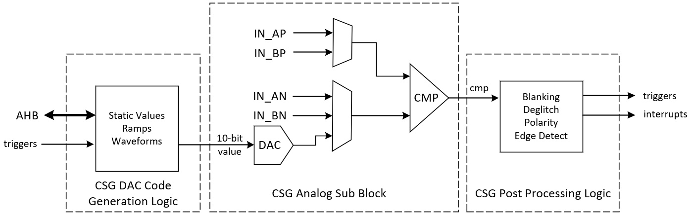
The user has various options to control the DAC data:
DAC data update can be triggered by either a HW or FW trigger. Available HW DAC trigger sources:
The Comparator can be configured to compare a signal from the dedicated analog input or from the DAC output to another selected analog input.
The CSG comparator output signal has the following post-processing options:
The HPPASS CSG block provides DAC and comparator interrupts to the CPU interrupt controller.
A DAC interrupt is generated on the following events:
The DAC interrupts should be enabled by setting the corresponding mask in the HPPASS_CSG_DAC_INTR_MASK register using Cy_HPPASS_DAC_SetInterruptMask function. To determine which DAC slice generated the interrupt, read the HPPASS_CSG_DAC_INTR_MASKED register using Cy_HPPASS_DAC_GetInterruptStatusMasked function. To clear the DAC interrupt, use Cy_HPPASS_DAC_ClearInterrupt function.
The CSG provides both individual interrupts for each of the five DAC slices (pass_interrupt_csg_dac_0..4_IRQn) and a combined DAC interrupt (pass_interrupt_csg_dacs_IRQn). When using the combined interrupt, the HPPASS_CSG_DAC_INTR register must be read using Cy_HPPASS_DAC_GetInterruptStatus function to determine the cause of the interrupt.
The CSG comparators provide only a combined interrupt.
The comparator interrupt can be generated on rising, falling, or both edges of the comparator output. The edge selection is configured in the comparator configuration structure cy_stc_hppass_comp_t::edge field. The selected comparator interrupt should be enabled by setting the corresponding mask in the HPPASS_CSG_CMP_INTR_MASK register using Cy_HPPASS_Comp_SetInterruptMask function. To determine which comparator generated the interrupt, read the HPPASS_CSG_CMP_INTR_MASKED register using Cy_HPPASS_Comp_GetInterruptStatusMasked function. To clear the comparator interrupt, use Cy_HPPASS_Comp_ClearInterrupt function.
To configure the CSG, the driver uses a configuration structure of type cy_stc_hppass_csg_t that must be predefined. This structure holds the pointer to the array of CSG slices configuration structures cy_stc_hppass_slice_t, as well the pointer to the array of the CSG LUT configuration structures cy_stc_hppass_lut_t. Also, this structure contains the DAC output selector field cy_en_hppass_dac_out_t, which routes the selected DAC output to the HPPASS SAR input for debugging purposes.
Each instance of the cy_stc_hppass_slice_t contains the comparator configuration structure cy_stc_hppass_comp_t and the DAC configuration structure cy_stc_hppass_dac_t.
Refer to the Technical Reference Manual for detailed information.
The example below shows how to configure the CSG slice to generate PWM signal on P7_0 with the duty cycle proportional to the analog input voltage on the AN_A0 pin.
API Reference | |
| Macros | |
| Functions | |
| Data Structures | |
| Enumerated Types | |