This driver provides the API functions to configure the successive approximation register analog-to-digital converter (SAR ADC) subsystem of the Autonomous Analog.
The versatile SAR ADC is an analog-to-digital converter with a dual-core 12-bit successive approximation register. The SAR ADC (hereafter ADC) contains a High Speed (HS) Core that can operate in Active mode with the SRSS clock up to 80 MHz and a Low Power (LP) Core based on the 4.096 MHz LPOSC from the Autonomous Analog. The HS Core is not available in DeepSleep while the LP Core is available in all power modes.
- Note
- Only one core can be active at a time.
For more information on the ADC, refer to the device Architecture Technical Reference Manual (TRM).
For the exact location of the pins, see the device datasheet.
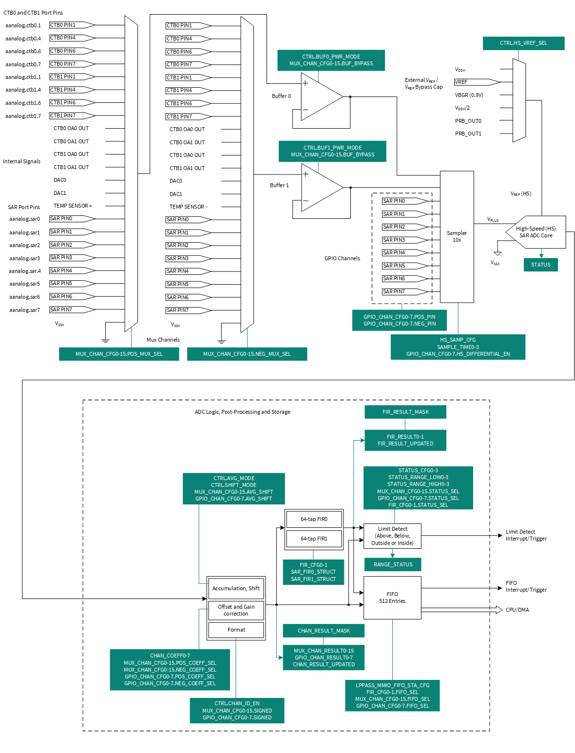
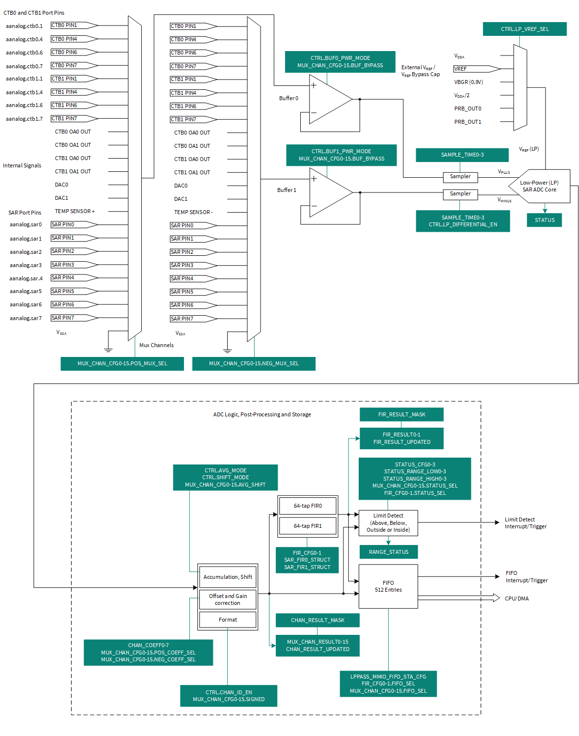
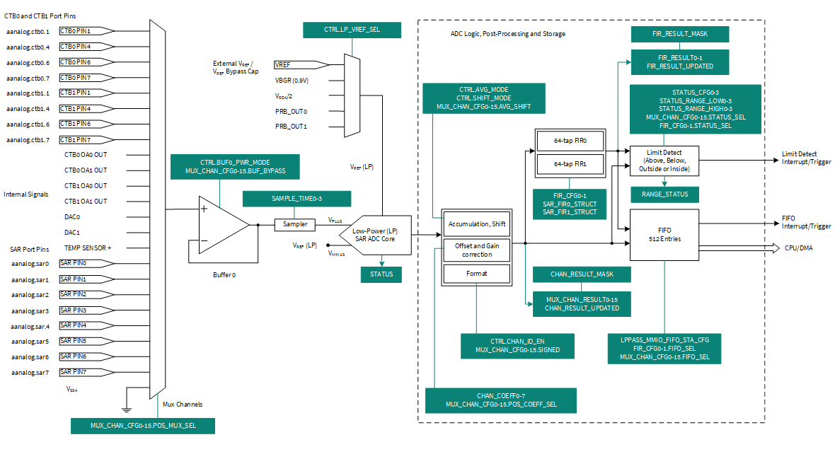
The key components of the ADC are:
- The inputs selector for routing signals from external pins (GPIO) or analog-capable internal IOs (MUX);
- A pair of Hi-Z buffers, which are in the MUX path only and can be bypassed;
- The sampler with sample and hold circuits (S/H) for simultaneous sampling from multiple sources:
- 8 single-ended S/H circuits directly connected to the GPIO and available in Active mode only;
- 2 single-ended S/H circuits connected to the MUX IOs and available in Active mode only;
- 1 fully differential sampler for all sources, available in Active and Deep Sleep modes;
- The source of reference voltages for HS/LP ADC Cores;
- Post-processing of the ADC output;
Channel Configuration
The signal path to the ADC input is controlled by the logical channel (a high-level abstraction). The configuration of the ADC logical channel includes the following settings (common for HS//LP modes):
Also:
8 individually-configurable logical channels are available to the ADC in HS mode and 16 logical channels are available to the ADC in LP mode.
The logical channels configuration is a part of the ADC Static Configuration (refer to cy_stc_autanalog_sar_sta_hs_t::hsGpioChan for GPIO inputs and cy_stc_autanalog_sar_sta_t::intMuxChan for MUX inputs accordingly).
Static Configuration
The static configuration contains application-specific settings intended to remain static for any ADC application. The Autonomous Controller (AC) will NOT change the static configuration during operation.
The diagram below shows the static configuration for ADC in HS mode.
The diagram below shows the static configuration for ADC in LP mode.
The diagram below shows the static configuration for LP ADC in Single Ended mode.
The static configuration for the whole ADC consists of static configurations for the HS and LP parts (refer to cy_stc_autanalog_sar_sta_hs_t, cy_stc_autanalog_sar_sta_lp_t) and includes the following settings in total (refer to cy_stc_autanalog_sar_sta_t):
Also:
Sequencer and State Transition Table
The sequencer is used to control the ADC to perform an automatic scan on all enabled logical channels without MCU intervention. Each ADC Core has its own sequencer, refer to cy_stc_autanalog_sar_seq_tab_hs_t for HS mode and refer to cy_stc_autanalog_sar_seq_tab_lp_t for LP mode. Both sequencers contain up to 32 states. Each state of the sequencer defines a single step in the ADC scan.
The Autonomous Controller is able to trigger the ADC. It points to a particular step (Entry State) of the sequencer in runtime using the State Transition Table, refer to cy_stc_autanalog_stt_sar_t. The next step of the sequencer is defined in the nextAction field of the sequencer configuration structure (refer to e.g. cy_stc_autanalog_sar_seq_tab_hs_t::nextAction):
- NEXT - Go to the next sequencer state to proceed to the next step in a given ADC scan;
- ENTRY_ADDR - Assert the SAR_EOS condition and jump to Entry State for continuous ADC scanning;
- STOP - Assert the SAR_DONE and SAR_EOS conditions and go to Idle to indicate the end of a scan;
The remaining fields of the sequencer are (common for HS//LP modes):
Also, the HS sequencer allows you to configure the following:
Also, the LP sequencer allows you to configure the following:
The ADC scan can be started by the Autonomous Controller (AC) in runtime per settings provided in the sequencer (refer to cy_stc_autanalog_sar_seq_tab_hs_t, cy_stc_autanalog_sar_seq_tab_lp_t) and State Transition Table (refer to cy_stc_autanalog_stt_sar_t structure).
- Note
- When ADC is powered down, the ADC logic and FIRs are reset, ADC/FIR clocks are gated, and all ADC AC conditions are cleared. The ADC configuration and sequencer tables are retained. The FIFO status and content are not cleared, i.e. the FIFO contents can still be read if the ADC is disabled.
Clock and Throughput
The ADC in HS mode is clocked from the SRSS peripheral clock (Clk_HF9, up to 80MHz, refer to General Configuration Considerations) in chip Active mode using Peri 0 Clock Group 2 8-bit divider in the clock chain.
The ADC in LP mode is clocked from the local Low Power Oscillator (LPOSC, 4096kHz, refer to cy_en_autanalog_timer_clk_src_t) in chip Deep Sleep mode.
| ADC mode | Clock source | Clock frequency, MHz | Throughput, samples/s |
| High Speed | Clk_HF9 | 80 | 5Msps |
| Low Power | LPOSC | 4.096 | 200ksps |
Sample Time
The sample time can be set separately for each HS\LP ADC Cores.
For HS mode, enable this option in the corresponding ADC sequencer, refer to cy_stc_autanalog_sar_seq_tab_hs_t::sampleTimeEn, cy_stc_autanalog_sar_seq_tab_hs_t::sampleTime. And the selection of a particular value of the acquisition time is defined in the corresponding Static configuration, refer to cy_stc_autanalog_sar_sta_hs_t::hsSampleTime.
For LP mode, enable this option in the corresponding ADC sequencer, refer to cy_stc_autanalog_sar_seq_tab_lp_t::sampleTimeEn, cy_stc_autanalog_sar_seq_tab_lp_t::sampleTime. The selection of a particular value of the acquisition time is defined in the corresponding Static configuration, refer to cy_stc_autanalog_sar_sta_lp_t::lpSampleTime.
- Note
- 15us is the recommended sampling time for Die temperature measurement in LP mode.
-
12us is the recommended sampling time for Die temperature measurement in HS mode.
Reference Voltage
The level of the reference voltage can be defined separately for each HS\LP ADC Cores in the corresponding parts of the Static configuration, refer to cy_stc_autanalog_sar_sta_hs_t::hsVref and cy_stc_autanalog_sar_sta_lp_t::lpVref.
For the PRB configuration settings, refer to cy_stc_autanalog_prb_t structure.
- Note
- Vdda is 1.8V and Vbgr is 0.9V
Buffer Input and Output Ranges
The input range of the buffer can be rail-to-rail if the charge pump is enabled. Without the charge pump, the input range is 0 V to VDDA - 1.5 V. The output range of the buffer is typically 0.2 V to VDDA - 1.0 V. See the device datasheet for more details.
| Charge Pump | Input Range | Output Range |
| Enabled | 0 V to VDDA | 0.2 V to VDDA - 0.2 V |
| Disabled | 0 V to VDDA - 1.5 V | 0.2 V to VDDA - 1.0 V |
- Note
- The charge pump nominal clock is 4MHz
For the configuration settings, see cy_en_autanalog_sar_buf_pwr_t.
Signed/Unsigned Output
The ADC conversion result and the FIR//FIFO output are represented as 32-bit width integer, (zero or sign extended) regardless of the actual resolution of the ADC.
For the configuration settings, refer to cy_stc_autanalog_sar_hs_chan_t::sign and cy_stc_autanalog_sar_mux_chan_t::sign.
Handling of the Result
The results of the ADC conversion or FIR filtering can be stored with further notification about update, or sent directly to the FIFO buffer. To save the result for a specific logical channel or FIR filter, use the following settings in the Static configuration:
Averaging
The ADC subsystem includes an accumulator and shift registers to support the averaging at the hardware level.
To configure the averaging for the ADC conversion result, use:
FIR Filter
Two instances of the 64-tap FIR filters are available for the ADC post-processing.
The FIR filter configuration (refer to cy_stc_autanalog_sar_fir_cfg_t) includes:
Interrupts, Triggers and STT Events
The following internal events of the ADC can be configured to generate an interrupt or trigger or used as the STT event in the Autonomous Analog (refer to cy_en_autanalog_ac_out_trigger_mask_t and cy_en_autanalog_stt_ac_condition_t):
- SAR_EOS - Indicates the end of the scanning of the logical ADC channels by the sequencer;
- SAR_RESULT (interrupt only) - Indicates an updated ADC conversion result;
- SAR_DONE - Indicates that the sequencer stopped scanning the ADC;
- SAR_RANGE - Indicates range detection conditions;
- SAR_FIR_RESULT (interrupt only) - Indicates an updated FIR filter calculation result;
- SAR_BUSY (STT event only) - Indicates that the ADC is in conversion;
- SAR_FIR_DONE (STT event only) - Indicates an updated FIR filter result;
- SAR_FIFO_DONE (STT event only) - Indicates SAR_DONE ANDED with FIFO writing complete;
- SAR_FIR_FIFO_DONE (STT event only) - Indicates that the FIR filter result is sent to the FIFO;
Refer to Interrupts, Triggers and STT Events chapter for the FIFO events.
Sample use case: Die Temperature
#include "autanalog_sar.h"
{
.sign = true,
.buffBypass = true,
.accShift = false,
};
@ CY_AUTANALOG_FIFO_DISABLED
DISABLED.
Definition: cy_autanalog_sar.h:958
cy_en_autanalog_sar_pin_mux_t posPin
Positive pin assignment.
Definition: cy_autanalog_sar.h:1071
The MUX channel configuration structure, refer to Channel Configuration chapter.
Definition: cy_autanalog_sar.h:1070
@ CY_AUTANALOG_SAR_LIMIT_STATUS_DISABLED
The limit status is not used.
Definition: cy_autanalog_sar.h:742
@ CY_AUTANALOG_SAR_CH_COEFF_DISABLED
The channel correction coefficient not used.
Definition: cy_autanalog_sar.h:772
@ CY_AUTANALOG_SAR_PIN_MUX_TEMP_SENSOR
Temperature sensor.
Definition: cy_autanalog_sar.h:721
{
.hsSampleTime = {1023U, 0U, 0U, 0U},
.hsGpioChan = {NULL, NULL, NULL, NULL, NULL, NULL, NULL, NULL},
};
cy_en_autanalog_sar_vref_t hsVref
Select ADC voltage reference, refer to Reference Voltage chapter.
Definition: cy_autanalog_sar.h:1109
The part of the Static configuration for ADC HS mode, refer to Static Configuration chapter.
Definition: cy_autanalog_sar.h:1108
@ CY_AUTANALOG_SAR_VREF_VBGR
The ADC reference is VBGR.
Definition: cy_autanalog_sar.h:798
#define CY_AUTANALOG_SAR_CHAN_MASK_GPIO_DISABLED
The GPIO channels masks.
Definition: cy_autanalog_sar.h:469
{
.hsStaCfg = &sarStaHsCfg,
.chanID = false,
.shiftMode = false,
.intMuxChan = {&intMuxChan0, NULL, NULL, NULL, NULL, NULL, NULL, NULL, NULL, NULL, NULL, NULL, NULL, NULL, NULL, NULL},
.limitCond = {NULL, NULL, NULL, NULL},
};
#define CY_AUTANALOG_SAR_MASK_FIR_DISABLED
The FIR channels masks.
Definition: cy_autanalog_sar.h:542
cy_stc_autanalog_sar_sta_lp_t * lpStaCfg
LP part of static configuration.
Definition: cy_autanalog_sar.h:1154
The ADC static configuration structure, refer to Static Configuration chapter.
Definition: cy_autanalog_sar.h:1153
@ CY_AUTANALOG_SAR_CAL_DISABLED
Calibration disabled.
Definition: cy_autanalog_sar.h:891
@ CY_AUTANALOG_SAR_ACC_DISABLED
Average disabled.
Definition: cy_autanalog_sar.h:850
@ CY_AUTANALOG_SAR_BUF_PWR_OFF
The power mode for the buffer is OFF, the buffer is disabled.
Definition: cy_autanalog_sar.h:814
#define CY_AUTANALOG_SAR_CHAN_MASK_MUX0
The MUX channel 0.
Definition: cy_autanalog_sar.h:513
{
.sampleTimeEn = true,
.accEn = false,
};
uint8_t chanEn
GPIO channels enable mask, valid range 0x0...0xFF, see High Speed Channels and Masks macros.
Definition: cy_autanalog_sar.h:1202
The ADC Sequencer Table configuration structure for HS mode, refer to Sequencer and State Transition ...
Definition: cy_autanalog_sar.h:1201
@ CY_AUTANALOG_SAR_NEXT_ACTION_STATE_STOP
Stop, send SAR_EOS and SAR_DONE events and idle.
Definition: cy_autanalog_sar.h:904
@ CY_AUTANALOG_SAR_SAMPLE_TIME0
Sampling Timer 0.
Definition: cy_autanalog_sar.h:878
@ CY_AUTANALOG_SAR_ACC_CNT2
Set samples averaged to 2.
Definition: cy_autanalog_sar.h:861
#define CY_AUTANALOG_SAR_CHAN_CFG_MUX0_PSEUDO_DIFF
The MUX channel pseudo differential.
Definition: cy_autanalog_sar.h:484
#define CY_AUTANALOG_SAR_CHAN_CFG_MUX0
The MUX channels configurations.
Definition: cy_autanalog_sar.h:494
{
.hsSeqTabNum = 1U,
.hsSeqTabArr = &sarHsSeqTabCfg,
.lpSeqTabNum = 0U,
.lpSeqTabArr = NULL,
.firNum = 0U,
.firCfg = NULL,
.fifoCfg = NULL,
};
cy_stc_autanalog_sar_sta_t * sarStaCfg
The pointer to a static part of the ADC configuration.
Definition: cy_autanalog_sar.h:1303
The configuration structure to set up the entire ADC.
Definition: cy_autanalog_sar.h:1301
{
{
.enable = true,
.trigger = false,
.entryState = 0U,
},
{
.unlock = true,
.enable = true,
.trigger = false,
.entryState = 0U,
},
{
.unlock = true,
.enable = true,
.trigger = true,
.entryState = 0U,
},
{
.unlock = true,
.enable = true,
.trigger = false,
.entryState = 0U,
},
};
bool unlock
ADC Unlock:
Definition: cy_autanalog_sar.h:1332
The ADC section in the State Transition Table state.
Definition: cy_autanalog_sar.h:1331
cy_en_autanalog_status_t
Return the status for functions of the Autonomous Analog driver.
Definition: cy_autanalog_common.h:109
{
}
@ CY_AUTANALOG_SUCCESS
Initialization completed successfully.
Definition: cy_autanalog_common.h:110
cy_en_autanalog_status_t Cy_AutAnalog_SAR_LoadConfig(uint8_t sarIdx, const cy_stc_autanalog_sar_t *sarCfg)
Configures the ADC per provided settings.
Definition: cy_autanalog_sar.c:117
- Warning
- The first reading of the die temperature in HS mode may be incorrect.