PSoC 6 Peripheral Driver Library
SD Host (SD Host Controller)

General Description

This driver provides the user an easy method for accessing standard Host Controller Interface (HCI) registers and provides some simple functionality on top of the HCI for reading and writing data to an SD card, eMMc card or a SDIO device.

The functions and other declarations used in this driver are in cy_sd_host.h. You can include cy_pdl.h to get access to all functions and declarations in the PDL.

Features:

Unsupported Features:

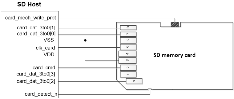
The SD, eMMC, and SDIO cards have the similar physical interface: clock, command line, and data lines. The SD card is removable and requires the SD card connector to connect to the PSoC device. This connector also has the card_mech_write_prot switch for mechanical write protection and the card_detect_n switch for card detection. The eMMC card also has DAT4-DAT7 pins for 8-bit mode and the EMMC_RESET pin.

sd_card_connector.png

The driver has a low-level and high-level APIs. The low-level functions provide an easy method to read and write registers. Also, these functions allow valid interaction with an SD Card, eMMC card, and SDIO card. The high-level functions provide an easy mechanism to enumerate a device, read, write, and erase data. They are RTOS-friendly. When starting a command, these functions do not wait until the command completes. The interrupt and flags are used to check when the transfer completes. This allows to put RTOS delays in the user code.

Configuration Considerations

The SD Host driver configuration can be divided to a number of sequential steps listed below:

Note
The SD Host driver is built on top of the SDHC hardware block. The SDHC1 instance is used as an example for all code snippets. Modify the code to match your design.

Enable SD Host

Enable the SDHC block calling Cy_SD_Host_Enable.

Assign and Configure Pins

Only dedicated SD Host pins can be used for SD Host operation. The HSIOM register must be configured to connect the block to the pins. Also, the SD Host pins must be configured in Strong Drive, Input buffer on:

/* Assign pins for SD Host on SDHC1 */
#define SDHC1_PORT1 (P12_0_PORT)
#define SDHC1_PORT2 (P13_0_PORT)
#define SDHC1_IO_VOLT_SEL_NUM (P12_7_NUM)
#define SDHC1_CARD_DETECT_N_NUM (P12_1_NUM)
#define SDHC1_CARD_MECH_WRITE_PROT_NUM (P12_2_NUM)
#define SDHC1_LED_CTRL_NUM (P12_3_NUM)
#define SDHC1_CARD_IF_PWR_EN_NUM (P12_6_NUM)
#define SDHC1_CARD_EMMC_RESET_N_NUM (P12_0_NUM)
#define SDHC1_CARD_CMD_NUM (P12_4_NUM)
#define SDHC1_CLK_CARD_NUM (P12_5_NUM)
#define SDHC1_CARD_DAT_3TO00_NUM (P13_0_NUM)
#define SDHC1_CARD_DAT_3TO01_NUM (P13_1_NUM)
#define SDHC1_CARD_DAT_3TO02_NUM (P13_2_NUM)
#define SDHC1_CARD_DAT_3TO03_NUM (P13_3_NUM)
/* Connect SD Host SDHC function to pins */
Cy_GPIO_SetHSIOM(SDHC1_PORT1, SDHC1_IO_VOLT_SEL_NUM, P12_7_SDHC1_IO_VOLT_SEL);
Cy_GPIO_SetHSIOM(SDHC1_PORT1, SDHC1_CARD_DETECT_N_NUM, P12_1_SDHC1_CARD_DETECT_N);
Cy_GPIO_SetHSIOM(SDHC1_PORT1, SDHC1_CARD_MECH_WRITE_PROT_NUM, P12_2_SDHC1_CARD_MECH_WRITE_PROT);
Cy_GPIO_SetHSIOM(SDHC1_PORT1, SDHC1_LED_CTRL_NUM, P12_3_SDHC1_LED_CTRL);
Cy_GPIO_SetHSIOM(SDHC1_PORT1, SDHC1_CARD_IF_PWR_EN_NUM, P12_6_SDHC1_CARD_IF_PWR_EN);
Cy_GPIO_SetHSIOM(SDHC1_PORT1, SDHC1_CARD_EMMC_RESET_N_NUM, P12_0_SDHC1_CARD_EMMC_RESET_N);
Cy_GPIO_SetHSIOM(SDHC1_PORT1, SDHC1_CARD_CMD_NUM, P12_4_SDHC1_CARD_CMD);
Cy_GPIO_SetHSIOM(SDHC1_PORT1, SDHC1_CLK_CARD_NUM, P12_5_SDHC1_CLK_CARD);
Cy_GPIO_SetHSIOM(SDHC1_PORT2, SDHC1_CARD_DAT_3TO00_NUM, P13_0_SDHC1_CARD_DAT_3TO00);
Cy_GPIO_SetHSIOM(SDHC1_PORT2, SDHC1_CARD_DAT_3TO01_NUM, P13_1_SDHC1_CARD_DAT_3TO01);
Cy_GPIO_SetHSIOM(SDHC1_PORT2, SDHC1_CARD_DAT_3TO02_NUM, P13_2_SDHC1_CARD_DAT_3TO02);
Cy_GPIO_SetHSIOM(SDHC1_PORT2, SDHC1_CARD_DAT_3TO03_NUM, P13_3_SDHC1_CARD_DAT_3TO03);
/* Configure pins for SDHC operation */
Cy_GPIO_SetDrivemode(SDHC1_PORT1, SDHC1_IO_VOLT_SEL_NUM, CY_GPIO_DM_STRONG);
Cy_GPIO_SetDrivemode(SDHC1_PORT1, SDHC1_CARD_DETECT_N_NUM, CY_GPIO_DM_STRONG);
Cy_GPIO_SetDrivemode(SDHC1_PORT1, SDHC1_CARD_MECH_WRITE_PROT_NUM, CY_GPIO_DM_STRONG);
Cy_GPIO_SetDrivemode(SDHC1_PORT1, SDHC1_LED_CTRL_NUM, CY_GPIO_DM_STRONG);
Cy_GPIO_SetDrivemode(SDHC1_PORT1, SDHC1_CARD_IF_PWR_EN_NUM, CY_GPIO_DM_STRONG);
Cy_GPIO_SetDrivemode(SDHC1_PORT1, SDHC1_CARD_EMMC_RESET_N_NUM, CY_GPIO_DM_STRONG);
Cy_GPIO_SetDrivemode(SDHC1_PORT1, SDHC1_CARD_CMD_NUM, CY_GPIO_DM_STRONG);
Cy_GPIO_SetDrivemode(SDHC1_PORT1, SDHC1_CLK_CARD_NUM, CY_GPIO_DM_STRONG);
Cy_GPIO_SetDrivemode(SDHC1_PORT2, SDHC1_CARD_DAT_3TO00_NUM, CY_GPIO_DM_STRONG);
Cy_GPIO_SetDrivemode(SDHC1_PORT2, SDHC1_CARD_DAT_3TO01_NUM, CY_GPIO_DM_STRONG);
Cy_GPIO_SetDrivemode(SDHC1_PORT2, SDHC1_CARD_DAT_3TO02_NUM, CY_GPIO_DM_STRONG);
Cy_GPIO_SetDrivemode(SDHC1_PORT2, SDHC1_CARD_DAT_3TO03_NUM, CY_GPIO_DM_STRONG);

Assign Clock Source

The SD Host is sourced from the CLK_HF clock. The clock must be set to 100 MHz:

/* Note: The CLK_HF2 input clock must be configured and enabled. */
/* Apply the CLK_HF2 divider to have CLK_HF2 = 100 MHz. */

Configure Interrupt (Optional)

The user can set up the interrupt for SD Host operation. The user is responsible for writing its own Interrupt handler. The Interrupt must be called in the interrupt handler for the selected SDHC instance. Also this interrupt must be enabled in the NVIC otherwise it will not work. It is the user's responsibility to clear the normal and error interrupt statuses. The interrupt statuses can be read using Cy_SD_Host_GetNormalInterruptStatus and Cy_SD_Host_GetErrorInterruptStatus. To clear the interrupt statuses, use Cy_SD_Host_ClearNormalInterruptStatus and Cy_SD_Host_ClearErrorInterruptStatus.

void SD_Host_User_Isr(void)
{
uint32_t normalStatus;
uint32_t errorStatus;
normalStatus = Cy_SD_Host_GetNormalInterruptStatus(SDHC1);
/* Check the Error event */
if (0u < normalStatus)
{
/* Clear the normalStatus event */
}
errorStatus = Cy_SD_Host_GetErrorInterruptStatus(SDHC1);
/* Check the Error event */
if (0u < errorStatus)
{
/* Clear the Error event */
}
/* Add the use code here. */
}
/* Assign SDHC1 interrupt number and priority */
#define SD_Host_INTR_NUM sdhc_1_interrupt_general_IRQn
#define SD_Host_INTR_PRIORITY (3UL)
/* Populate configuration structure (code specific for CM4) */
const cy_stc_sysint_t sdHostIntrConfig =
{
#if (CY_CPU_CORTEX_M0P)
/* .intrSrc */ NvicMux4_IRQn,
/* .cm0pSrc */ SD_Host_INTR_NUM,
#else
/* .intrSrc */ SD_Host_INTR_NUM, /* SD Host interrupt number (non M0 core)*/
#endif
/* .intrPriority */ SD_Host_INTR_PRIORITY
};
/* Generate an interrupt on SD card insertion or removal */
/* Enable global interrupts. */
__enable_irq();
/* Hook interrupt service routine and enable interrupt */
(void) Cy_SysInt_Init(&sdHostIntrConfig, &SD_Host_User_Isr);
#if (CY_CPU_CORTEX_M0P)
NVIC_EnableIRQ(NvicMux4_IRQn);
#else
NVIC_EnableIRQ(SD_Host_INTR_NUM);
#endif

Configure SD Host

To set up the SD Host driver, provide the configuration parameters in the cy_stc_sd_host_init_config_t structure. Set the emmc parameter to true for the eMMC-device, otherwise set it to false. Set dmaType if DMA mode is used for read/write operations. The other parameters are optional for operation. To initialize the driver, call the Cy_SD_Host_Init function providing a pointer to the filled cy_stc_sd_host_init_config_t structure and allocated cy_stc_sd_host_context_t.

/* Allocate context for SD Host operation */
/* Populate configuration structure */
const cy_stc_sd_host_init_config_t sdHostConfig =
{
.enableLedControl = false,
.emmc = false,
};
/* Configure SD Host to operate */
(void) Cy_SD_Host_Init(SDHC1, &sdHostConfig, &sdHostContext);

The SD, eMMC or SDIO card can be configured using the Cy_SD_Host_InitCard function as a pointer to the filled cy_stc_sd_host_sd_card_config_t structure and allocated cy_stc_sd_host_context_t.

Initialize the card

Finally, enable the card operation calling Cy_SD_Host_InitCard.

uint32_t rca;
/* Populate configuration structure */
{
.cardType = &cardType,
.rca = &rca,
.cardCapacity = &cardCapacity,
};
/* Initialize the card */
(void) Cy_SD_Host_InitCard(SDHC1, &sdCardConfig, &sdHostContext);

Common Use Cases

SD card Operation

The master API is divided into two categories: High-Level and Low-Level. Therefore, there are two methods for initiating SD card transactions using either Low-Level or High-Level API.

Use High-Level Functions

Call Cy_SD_Host_Read or Cy_SD_Host_Write to communicate with the SD memory device. These functions do not block in DMA mode and only start a transaction. After a transaction starts, the user should check the further data-transaction complete event. The example below shows sending and reading data in DMA mode.

/* Note: SD Host and the card must be initialized in ADMA2 or SDMA
* mode before using the code below.
*/
#define DATA (7U) /* Data to write. */
uint8_t rxBuff[CY_SD_HOST_BLOCK_SIZE]; /* Data to read. */
uint8_t txBuff[CY_SD_HOST_BLOCK_SIZE]; /* Data to write. */
memset(txBuff, DATA, sizeof(txBuff)); /* Fill the array with data to write. */
data.address = 0UL; /* The address to write/read data on the card or eMMC. */
data.numberOfBlocks = 1UL; /* The number of blocks to write/read (Single block write/read). */
data.autoCommand = CY_SD_HOST_AUTO_CMD_NONE; /* Selects which auto commands are used if any. */
data.dataTimeout = 12UL; /* The timeout value for the transfer. */
data.enReliableWrite = false; /* For EMMC cards enable reliable write. */
data.enableDma = true; /* Enable DMA mode. */
data.data = (uint32_t*)txBuff; /* The pointer to data to write. */
ret = Cy_SD_Host_Write(SDHC1, &data, &sdHostContext); /* Write data to the card. */
if (CY_SD_HOST_SUCCESS == ret)
{
{
/* Wait for the data-transaction complete event. */
}
}
data.data = (uint32_t*)rxBuff; /* The pointer to data to read. */
ret = Cy_SD_Host_Read(SDHC1, &data, &sdHostContext); /* Read data from the card. */
if (CY_SD_HOST_SUCCESS == ret)
{
{
/* Wait for the data-transaction complete event. */
}
/* Clear the data-transaction complete event. */
Cy_SD_Host_ClearNormalInterruptStatus(SDHC1, CY_SD_HOST_XFER_COMPLETE);
}

Use Low-Level Functions

Call Cy_SD_Host_InitDataTransfer to initialize the SD block for a data transfer. It does not start a transfer. To start a transfer call Cy_SD_Host_SendCommand after calling this function. If DMA is not used for Data transfer then the buffer needs to be filled with data first if this is a write. Wait the transfer complete event. ADMA3 mode requires calling Cy_SD_Host_InitDataTransfer to initialize the DMA transaction. The ADMA3 mode example is shown below.

/* The code below demonstrates ADMA3 mode for writing
* two buffers of data in two different addresses in
* the card and reading data from the card into one buffer.
* All these operations are performed using one DMA transaction.
* Each Write buffer has the length of two blocks (1024 bytes).
* The first txBuff_1 buffer contains 0x01 values and
* the second txBuff_2 buffer contains 0x03 values.
* The txBuff_1 data is written to the address = 0 using
* the CMD25 command. The txBuff_2 data is written to
* the address = 2 (or 1024 for SDSC cards) using the
* CMD25 command. The Read buffer has the length of
* four blocks (2048 bytes). The rxBuff data is read from
* the address = 0 using the CMD18 command
* (Read data should contain all data from two Write buffers).
*/
/* Note: SD Host and the card must be initialized in ADMA3 mode before
* using the code below.
*/
#define WR_BLOCK_NUM (2UL) /* Number of blocks to write */
#define RD_BLOCK_NUM (4UL) /* Number of blocks to read */
#define VALUE1 (0x1U) /* Value to write into first two blocks */
#define VALUE2 (0x3U) /* Value to write into last two blocks */
uint32_t integratedDescriptor[6]; /* Integrated Descriptor */
uint32_t cmdDescriptor0[10]; /* Command Descriptor for CMD25 */
uint32_t cmdDescriptor1[10]; /* Command Descriptor for CMD25 */
uint32_t cmdDescriptor2[10]; /* Command Descriptor for CMD18 */
uint8_t txBuff_1[CY_SD_HOST_BLOCK_SIZE*WR_BLOCK_NUM]; /* The first buffer to write data */
uint8_t txBuff_2[CY_SD_HOST_BLOCK_SIZE*WR_BLOCK_NUM]; /* The second buffer to write data */
uint8_t rxBuff[CY_SD_HOST_BLOCK_SIZE*RD_BLOCK_NUM]; /* The buffer to read data */
uint32_t wrRdAddress = 0UL; /* Write Address 1 (and read address)*/
uint32_t wrAddress2 = WR_BLOCK_NUM; /* Write Address 2 */
cy_stc_sd_host_data_config_t dataConfig; /* The data configuration structure */
/* Fill the buffers */
memset(txBuff_1, VALUE1, sizeof(txBuff_1));
memset(txBuff_2, VALUE2, sizeof(txBuff_2));
memset(rxBuff, 0UL, sizeof(rxBuff));
/* The SDSC cards have byte addressing. The SDHC/SDXC cards have block addressing.
* The address should be multiplied by 512 for the SDSC cards.
*/
if (CY_SD_HOST_SDSC == sdHostContext.cardCapacity)
{
wrRdAddress = wrRdAddress << CY_SD_HOST_SDSC_ADDR_SHIFT;
wrAddress2 = wrAddress2 << CY_SD_HOST_SDSC_ADDR_SHIFT;
}
/* Configure read/write structure. enableDma = true and
* ADMA3 Integrated Descriptor Address are enough for ADMA3 mode.
*/
dataConfig.enableDma = true;
dataConfig.data = (uint32_t*)&integratedDescriptor[0];
/* Make sure that descriptors are empty */
memset(integratedDescriptor, 0UL, sizeof(integratedDescriptor));
memset(cmdDescriptor0, 0UL, sizeof(cmdDescriptor0));
memset(cmdDescriptor1, 0UL, sizeof(cmdDescriptor1));
memset(cmdDescriptor2, 0UL, sizeof(cmdDescriptor2));
/* The Integrated Descriptor */
integratedDescriptor[0] = 1UL << CY_SD_HOST_ADMA_ATTR_VALID_POS | /* Attr Valid */
0UL << CY_SD_HOST_ADMA_ATTR_END_POS | /* Attr End */
0UL << CY_SD_HOST_ADMA_ATTR_INT_POS | /* Attr Int */
0UL << CY_SD_HOST_ADMA_LEN_POS; /* Len */
integratedDescriptor[1] = (uint32_t)&cmdDescriptor0[0];
integratedDescriptor[2] = 1UL << CY_SD_HOST_ADMA_ATTR_VALID_POS | /* Attr Valid */
0UL << CY_SD_HOST_ADMA_ATTR_END_POS | /* Attr End */
0UL << CY_SD_HOST_ADMA_ATTR_INT_POS | /* Attr Int */
0UL << CY_SD_HOST_ADMA_LEN_POS; /* Len */
integratedDescriptor[3] = (uint32_t)&cmdDescriptor1[0];
integratedDescriptor[4] = 1UL << CY_SD_HOST_ADMA_ATTR_VALID_POS | /* Attr Valid */
1UL << CY_SD_HOST_ADMA_ATTR_END_POS | /* Attr End */
0UL << CY_SD_HOST_ADMA_ATTR_INT_POS | /* Attr Int */
0UL << CY_SD_HOST_ADMA_LEN_POS; /* Len */
integratedDescriptor[5] = (uint32_t)&cmdDescriptor2[0];
/* The Command Descriptor for SD Mode - Write to first two blocks */
/* 32-bit Block Count */
cmdDescriptor0[0] = 1UL << CY_SD_HOST_ADMA_ATTR_VALID_POS | /* Attr Valid */
0UL << CY_SD_HOST_ADMA_ATTR_END_POS | /* Attr End */
0UL << CY_SD_HOST_ADMA_ATTR_INT_POS | /* Attr Int */
0UL << CY_SD_HOST_ADMA_LEN_POS; /* Len */
cmdDescriptor0[1] = WR_BLOCK_NUM; /* number Of Block */
/* (16-bit Block Count) + Block Size */
cmdDescriptor0[2] = 1UL << CY_SD_HOST_ADMA_ATTR_VALID_POS | /* Attr Valid */
0UL << CY_SD_HOST_ADMA_ATTR_END_POS | /* Attr End */
0UL << CY_SD_HOST_ADMA_ATTR_INT_POS | /* Attr Int */
0UL << CY_SD_HOST_ADMA_LEN_POS; /* Len */
cmdDescriptor0[3] = CY_SD_HOST_BLOCK_SIZE; /* block Size */
/* Argument */
cmdDescriptor0[4] = 1UL << CY_SD_HOST_ADMA_ATTR_VALID_POS | /* Attr Valid */
0UL << CY_SD_HOST_ADMA_ATTR_END_POS | /* Attr End */
0UL << CY_SD_HOST_ADMA_ATTR_INT_POS | /* Attr Int */
0UL << CY_SD_HOST_ADMA_LEN_POS; /* Len */
cmdDescriptor0[5] = wrRdAddress; /* Write Address 1 */
/* Command + Transfer Mode */
cmdDescriptor0[6] = 1UL << CY_SD_HOST_ADMA_ATTR_VALID_POS | /* Attr Valid */
0UL << CY_SD_HOST_ADMA_ATTR_END_POS | /* Attr End */
0UL << CY_SD_HOST_ADMA_ATTR_INT_POS | /* Attr Int */
0UL << CY_SD_HOST_ADMA_LEN_POS; /* Len */
cmdDescriptor0[7] = 25UL << (16U + 0x8U) | /* Command Index - CMD25 */
1UL << (16U + 0x5U) | /* Data Present Select */
1UL << (16U + 0x4U) | /* Index Check Enable */
1UL << (16U + 0x3U) | /* CRC Check Enable */
CY_SD_HOST_RESPONSE_LEN_48 << (16U + 0x0U) | /* Response Type Select */
1UL << (0x5U) | /* Multi block/single block Select */
0UL << (0x4U) | /* 1 - read, 0 - write */
CY_SD_HOST_AUTO_CMD_12 << (0x2U) | /* Auto CMD enable */
1UL << (0x1U) | /* Block count enable */
1UL << (0x0U) | /* DMA enable */
1UL << (0x8U); /* Response Interrupt Disable */
/* The DMA2 Descriptor */
cmdDescriptor0[8] = 1UL << CY_SD_HOST_ADMA_ATTR_VALID_POS | /* Attr Valid */
1UL << CY_SD_HOST_ADMA_ATTR_END_POS | /* Attr End */
0UL << CY_SD_HOST_ADMA_ATTR_INT_POS | /* Attr Int */
(CY_SD_HOST_BLOCK_SIZE * WR_BLOCK_NUM) << CY_SD_HOST_ADMA_LEN_POS; /* Len */
cmdDescriptor0[9] = (uint32_t)&txBuff_1; /* Address */
/* The Command Descriptor for SD Mode - Write to second two blocks */
/* 32-bit Block Count */
cmdDescriptor1[0] = 1UL << CY_SD_HOST_ADMA_ATTR_VALID_POS | /* Attr Valid */
0UL << CY_SD_HOST_ADMA_ATTR_END_POS | /* Attr End */
0UL << CY_SD_HOST_ADMA_ATTR_INT_POS | /* Attr Int */
0UL << CY_SD_HOST_ADMA_LEN_POS; /* Len */
cmdDescriptor1[1] = WR_BLOCK_NUM; /* number Of Block */
/* (16-bit Block Count) + Block Size */
cmdDescriptor1[2] = 1UL << CY_SD_HOST_ADMA_ATTR_VALID_POS | /* Attr Valid */
0UL << CY_SD_HOST_ADMA_ATTR_END_POS | /* Attr End */
0UL << CY_SD_HOST_ADMA_ATTR_INT_POS | /* Attr Int */
0UL << CY_SD_HOST_ADMA_LEN_POS; /* Len */
cmdDescriptor1[3] = CY_SD_HOST_BLOCK_SIZE; /* block Size */
/* Argument */
cmdDescriptor1[4] = 1UL << CY_SD_HOST_ADMA_ATTR_VALID_POS | /* Attr Valid */
0UL << CY_SD_HOST_ADMA_ATTR_END_POS | /* Attr End */
0UL << CY_SD_HOST_ADMA_ATTR_INT_POS | /* Attr Int */
0UL << CY_SD_HOST_ADMA_LEN_POS; /* Len */
cmdDescriptor1[5] = wrAddress2; /* Write Address 2 */
/* Command + Transfer Mode */
cmdDescriptor1[6] = 1UL << CY_SD_HOST_ADMA_ATTR_VALID_POS | /* Attr Valid */
0UL << CY_SD_HOST_ADMA_ATTR_END_POS | /* Attr End */
0UL << CY_SD_HOST_ADMA_ATTR_INT_POS | /* Attr Int */
0UL << CY_SD_HOST_ADMA_LEN_POS; /* Len */
cmdDescriptor1[7] = 25UL << (16U + 0x8U) | /* Command Index - CMD25 */
1UL << (16U + 0x5U) | /* Data Present Select */
1UL << (16U + 0x4U) | /* Index Check Enable */
1UL << (16U + 0x3U) | /* CRC Check Enable */
CY_SD_HOST_RESPONSE_LEN_48 << (16U + 0x0U) | /* Response Type Select */
1UL << (0x5U) | /* Multi block/single block Select */
0UL << (0x4U) | /* 1 - read, 0 - write */
CY_SD_HOST_AUTO_CMD_12 << (0x2U) | /* Auto CMD enable */
1UL << (0x1U) | /* Block count enable */
1UL << (0x0U) | /* DMA enable */
1UL << (0x8U); /* Response Interrupt Disable */
/* The DMA2 Descriptor */
cmdDescriptor1[8] = 1UL << CY_SD_HOST_ADMA_ATTR_VALID_POS | /* Attr Valid */
1UL << CY_SD_HOST_ADMA_ATTR_END_POS | /* Attr End */
0UL << CY_SD_HOST_ADMA_ATTR_INT_POS | /* Attr Int */
(CY_SD_HOST_BLOCK_SIZE * WR_BLOCK_NUM) << CY_SD_HOST_ADMA_LEN_POS; /* Len */
cmdDescriptor1[9] = (uint32_t)&txBuff_2; /* Address */
/* The Command Descriptor for SD Mode - Read all four blocks */
/* 32-bit Block Count */
cmdDescriptor2[0] = 1UL << CY_SD_HOST_ADMA_ATTR_VALID_POS | /* Attr Valid */
0UL << CY_SD_HOST_ADMA_ATTR_END_POS | /* Attr End */
0UL << CY_SD_HOST_ADMA_ATTR_INT_POS | /* Attr Int */
0UL << CY_SD_HOST_ADMA_LEN_POS; /* Len */
cmdDescriptor2[1] = RD_BLOCK_NUM; /* number Of Block */
/* (16-bit Block Count) + Block Size */
cmdDescriptor2[2] = 1UL << CY_SD_HOST_ADMA_ATTR_VALID_POS | /* Attr Valid */
0UL << CY_SD_HOST_ADMA_ATTR_END_POS | /* Attr End */
0UL << CY_SD_HOST_ADMA_ATTR_INT_POS | /* Attr Int */
0UL << CY_SD_HOST_ADMA_LEN_POS; /* Len */
cmdDescriptor2[3] = CY_SD_HOST_BLOCK_SIZE; /* block Size */
/* Argument */
cmdDescriptor2[4] = 1UL << CY_SD_HOST_ADMA_ATTR_VALID_POS | /* Attr Valid */
0UL << CY_SD_HOST_ADMA_ATTR_END_POS | /* Attr End */
0UL << CY_SD_HOST_ADMA_ATTR_INT_POS | /* Attr Int */
0UL << CY_SD_HOST_ADMA_LEN_POS; /* Len */
cmdDescriptor2[5] = wrRdAddress; /* Read address */
/* Command + Transfer Mode */
cmdDescriptor2[6] = 1UL << CY_SD_HOST_ADMA_ATTR_VALID_POS | /* Attr Valid */
0UL << CY_SD_HOST_ADMA_ATTR_END_POS | /* Attr End */
0UL << CY_SD_HOST_ADMA_ATTR_INT_POS | /* Attr Int */
0UL << CY_SD_HOST_ADMA_LEN_POS; /* Len */
cmdDescriptor2[7] = 18UL << (16U + 0x8U) | /* Command Index - CMD18 */
1UL << (16U + 0x5U) | /* Data Present Select */
1UL << (16U + 0x4U) | /* Index Check Enable */
1UL << (16U + 0x3U) | /* CRC Check Enable */
CY_SD_HOST_RESPONSE_LEN_48 << (16U + 0x0U) | /* Response Type Select */
1UL << (0x5U) | /* Multi block/single block Select */
1UL << (0x4U) | /* 1 - read, 0 - write */
CY_SD_HOST_AUTO_CMD_12 << (0x2U) | /* Auto CMD enable */
1UL << (0x1U) | /* Block count enable */
1UL << (0x0U) | /* DMA enable */
1UL << (0x8U); /* Response Interrupt Disable */
/* The DMA2 Descriptor */
cmdDescriptor2[8] = 1UL << CY_SD_HOST_ADMA_ATTR_VALID_POS | /* Attr Valid */
1UL << CY_SD_HOST_ADMA_ATTR_END_POS | /* Attr End */
0UL << CY_SD_HOST_ADMA_ATTR_INT_POS | /* Attr Int */
(CY_SD_HOST_BLOCK_SIZE * RD_BLOCK_NUM) << CY_SD_HOST_ADMA_LEN_POS; /* Len */
cmdDescriptor2[9] = (uint32_t)&rxBuff; /* Address */
/* Initialize ADMA3 Data Transfer */
status = Cy_SD_Host_InitDataTransfer(SDHC1, &dataConfig);
if (CY_SD_HOST_SUCCESS == status)
{
{
/* Wait for the data-transaction complete event. */
}
/* Clear the data-transaction complete event. */
Cy_SD_Host_ClearNormalInterruptStatus(SDHC1, CY_SD_HOST_XFER_COMPLETE);
}

eMMC Card Operation

eMMC cards use the same API for writing and reading data. Additionally, eMMC requires configuring GPIO pins for DAT signals in 8-bit mode and card_emmc_reset_n pin if needed. The emmc member of cy_stc_sd_host_init_config_t structure must be set to "true".

eMMC SDIO or Combo Card Operation

Cy_SD_Host_InitCard() initializes all types of cards and automatically detects the card type: SD, SDIO or Combo card. SDIO cards have their input-output (I/O) functions that can be controlled using the GPIO driver. Combo Cards can use both I/O and memory API.

Low Power Support

The SD Host does not operate in Hibernate and Deep Sleep modes but it can automatically continue write/read operation after restoring from Deep Sleep mode. SD CLK must be disabled before going to Deep Sleep mode and can be enabled after wake up from Deep Sleep mode. To reduce the power consumption in Active mode, the user can stop the clock of the SD bus but the following interrupts can be allowed: Card Insert, Card Removal and SDIO Interrupt.

SD Card Removal and Insertion

SD card removal or insertion can be detected by calling Cy_SD_Host_GetNormalInterruptStatus which returns the card removal or card insertion events (CY_SD_HOST_CARD_REMOVAL or CY_SD_HOST_CARD_INSERTION bits). These events should be reset using Cy_SD_Host_ClearNormalInterruptStatus when they occur. When the card is removed, the SDHC block disables the CMD/DAT output. It is recommended to set DAT pins to the Digital High-Z (CY_GPIO_DM_HIGHZ) drive mode when card removal is detected. This can be doing using the GPIO driver. When the card is inserted, the SDHC block automatically disables the card power and clock. After card insertion, the user should set the DAT pins drive mode back to Strong Drive, Input buffer on (CY_GPIO_DM_STRONG), and then call Cy_SD_Host_InitCard.

Note
If CARD_INTERRUPT is enabled and DAT pins are not set to Digital High-Z drive mode then the interrupt will continuously trigger because the DAT1 line is driven low upon card re-insertion. The user will have to detect the card removal in the ISR handler, apply the power to the card using Cy_SD_Host_EnableCardVoltage, set to the DAT pins drive mode to the Digital High-Z (CY_GPIO_DM_HIGHZ) and clear CY_SD_HOST_CARD_INTERRUPT bit using Cy_SD_Host_ClearNormalInterruptStatus.

Low Voltage Signaling

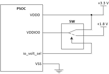
When lowVoltageSignaling is true, the SD Host driver sets UHS-I mode during the card initialization. The SD Host driver always starts talking to the card at 3.3V and then later switches to 1.8V. There is no internal regulator in the PSoC 6 to change SD signals from 3.3V to 1.8V. Thus, an external regulator is needed for the VDDIO of the PSoC device to provide the ability to go from 3.3V to 1.8V. The SD Host driver sets the io_volt_sel pin to high which is used to control the external regulator.

sd_host_low_voltage_signaling.png

More Information

Refer to the appropriate device technical reference manual (TRM) for a detailed description of the registers.

MISRA-C Compliance

MISRA Rule Rule Class (Required/Advisory) Rule Description Description of Deviation(s)
11.4 A A cast should not be performed between a pointer to object type and a different pointer to object type. The function Cy_SD_Host_DeepSleepCallback is the callback of the cy_en_syspm_status_t type. The cast operation safety in these functions becomes the user's responsibility because pointers are initialized when the callback is registered in the SysPm driver.
20.3 R The validity of values passed to library functions shall be checked. This violation is not caused by code changes, i.e. is not a regression.

Changelog

VersionChangesReason for Change
1.50.1 Minor documentation updates. Documentation enhancement.
1.50 The default value of the SD-clock rump-up time during a wakeup from Deep Sleep is reduced to 1 us, for details, see Cy_SD_Host_DeepSleepCallback description. Optimization for cases of specific wakeup timing requirements.
1.40 Added a possibility to customize the SD-clock rump-up time during a wakeup from Deep Sleep, for details, see Cy_SD_Host_DeepSleepCallback description. Workaround for cases of specific wakeup timing requirements.
1.30 The internal function implementation is changed. Code efficiency enhancement, minor defect fixing.
1.20 Added the Cy_SD_Host_DeepSleepCallback() function. Driver maintenance.
Fixed the Cy_SD_Host_GetCsd() function behaviour. Now the cy_stc_sd_host_context_t::maxSectorNum is being updated correctly Defect fixing.
1.10.1 Documentation of the MISRA rule violation. MISRA compliance.
1.10 The PLL and CLK disable sequence in Cy_SD_Host_DisableSdClk() is changed to disable CLK first.
The Low-Power Support section is updated with additional information about disabling CLK.
The context initialization in Cy_SD_Host_Init() is corrected.
Updated the Write/Read sequence in Cy_SD_Host_Read() and functions for non DMA mode.
Defect fixing.
1.0 The initial version.

API Reference

 Macros
 
 Functions
 
 Data Structures
 
 Enumerated Types