 |
PSoC 6 Peripheral Driver Library
|
|
PSoC 6 Peripheral Driver Library
|
The CTDAC driver provides APIs to configure the 12-bit Continuous-Time DAC.
The functions and other declarations used in this driver are in cy_ctdac.h. You can include cy_pdl.h to get access to all functions and declarations in the PDL.
The CTDAC generates a 12-bit DAC output voltage from the reference. The DAC reference can come from VDDA or from any signal buffered through Opamp0 of the CTB. This can be an external signal through a GPIO or from the internal AREF. The CTDAC is closely integrated with the CTB block, which provides easy buffering of the DAC output voltage, buffered input reference voltage, and sample and hold for the DAC output. The CTDAC control interface provides control of the DAC output through CPU or DMA. This includes a double-buffered DAC voltage control register, clock input for programmable update rate, interrupt on DAC buffer empty, and trigger to DMA.
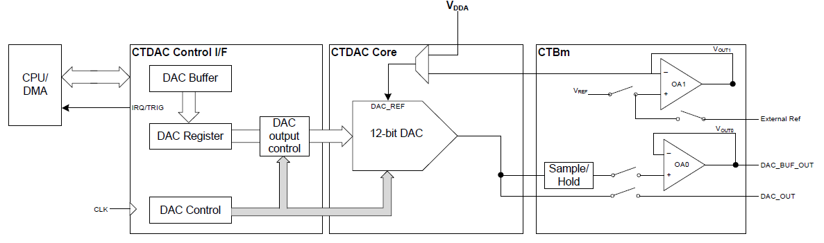
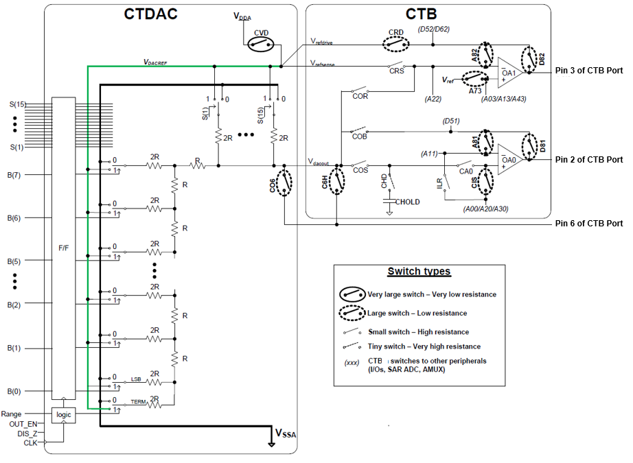
The CTDAC has two switches, CO6 for configuring the output path and CVD for the reference source.
Configure the CTDAC hardware block by calling Cy_CTDAC_Init. The base address of the CTDAC hardware can be found in the device-specific header file. If the buffers in the CTB are used for the reference source or the output, initialize the CTB hardware block. After both blocks are initialized, enable the CTB block before enabling the CTDAC block.
The driver also provides a Cy_CTDAC_FastInit function for fast and easy initialization of the CTDAC. The driver has pre-defined configuration structures for the four combinations of the reference and output buffers.
After initialization, call Cy_CTDAC_Enable to enable the hardware.
The CTDAC contains two registers:
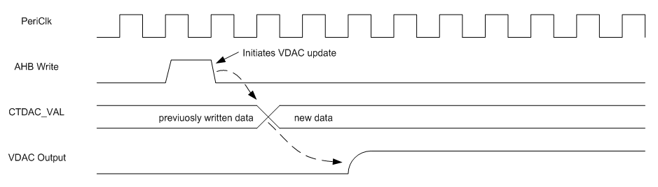
CTDAC_VAL
For direct firmware writes to update the current DAC value immediately. This register is written with Cy_CTDAC_SetValue.
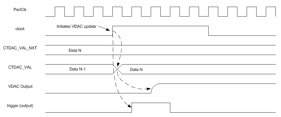
CTDAC_VAL_NXT
For buffered writes to update the DAC value at a periodic rate or with a strobe trigger input. This register is written with Cy_CTDAC_SetValueBuffered.
The update mode is selected during initialization with the cy_stc_ctdac_config_t::updateMode. Four of these modes require a dedicated clock resource and the driver can configure the clock during initialization (see cy_stc_ctdac_config_t).
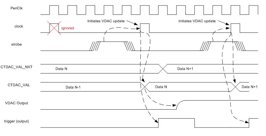
Three of these modes use a strobe signal through the digital signal interface (DSI). This allows control of the buffered update timing from an external source, for example, by another chip peripheral or from an off-chip source.
In this mode, the user writes directly into the CTDAC_VAL register using Cy_CTDAC_SetValue. The action of writing to this register will update the DAC output. This mode does not generate an interrupt or trigger signal. In this mode, a clock must not be configured. Additionally, calling Cy_CTDAC_SetValueBuffered does not update the DAC output.
In this mode, the user writes to the CTDAC_VAL_NXT register using Cy_CTDAC_SetValueBuffered. The rising edge of the clock will update the DAC output and generate the interrupt and trigger signals.
Whenever data is transferred from the CTDAC_VAL_NXT register, an interrupt is asserted the same time as the trigger. But while the trigger is automatically cleared after two PeriClk cycles, the user must clear the interrupt with Cy_CTDAC_ClearInterrupt.
In this mode, the user writes to the CTDAC_VAL_NXT register using Cy_CTDAC_SetValueBuffered. Each rising edge of the DSI strobe input enables one subsequent update from the next rising edge of the clock. The DSI input must remain high for two PeriClk cycles and go low for another two PeriClk cycles to allow for the next update. This restricts the DSI strobe input frequency to the PeriClk frequency divided by four.
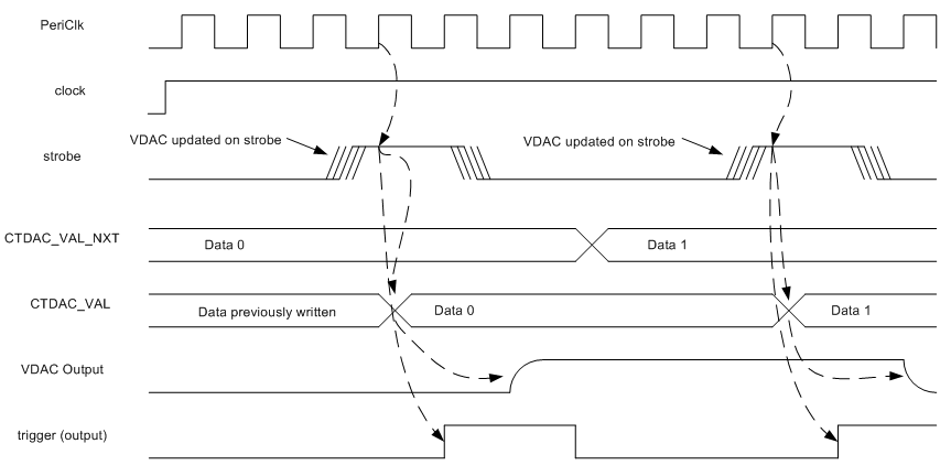
In this mode, the user writes to the CTDAC_VAL_NXT register using Cy_CTDAC_SetValueBuffered. The clock resource is used but set to a logic high. Therefore, each rising edge of the DSI strobe input immediately updates the DAC output.
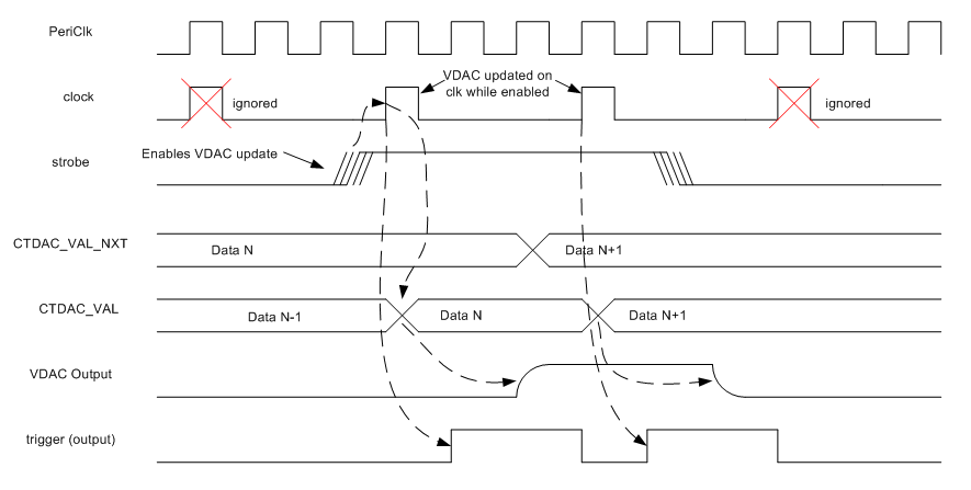
In this mode, the user writes to the CTDAC_VAL_NXT register using Cy_CTDAC_SetValueBuffered. The DSI strobe input acts as a hardware enable signal. While the DSI strobe input is high, the mode behaves like the Buffered write mode. When the DSI strobe input is low, updates are disabled.
The format of code stored in the CTDAC_VAL register can either be unsigned or signed two's complemented. Only the first 12 bits of the register are used by the DAC so there is no need for sign extension. With the signed format, the DAC decodes the code in the register by adding 0x800. The DAC can output the register value or the register value plus 1 (see Cy_CTDAC_SetOutputMode).
| 12-bit unsigned code | 12-bit two's complement signed code | Vout (for CY_CTDAC_OUTPUT_VALUE ) | Vout (for CY_CTDAC_OUTPUT_VALUE_PLUS1 ) |
|---|---|---|---|
| 0x000 | 0x800 | 0 | Vref/4096 |
| 0x800 | 0x000 | 0.5 * Vref | Vref * 2049 / 4096 |
| 0xFFF | 0x7FF | Vref * 4095 / 4096 | Vref |
The expressions in the above table are based on an unbuffered DAC output. When the output is buffered, the input and output range of the buffer will affect the output voltage. See Opamp Input and Output Range in the CTB driver for more information.
When data from the CTDAC_VAL_NXT is transferred to the CTDAC_VAL register, an interrupt and trigger output are generated. The trigger output can be used with a DMA block to update the CTDAC value register at high speeds without any CPU intervention. Alternatively, the interrupt output can be used when DMA is not available to update the CTDAC value register, but at a slower speed.
Recall with the Update Modes, the interrupt and trigger output are available in all modes except Direct write.
The CTDAC trigger output signal can be routed to a DMA block using the TrigMux (Trigger Multiplexer) to trigger an update to the CTDAC_VAL_NXT register. When making the required Cy_TrigMux_Connect calls, use the pre-defined enums, TRIG14_IN_PASS_TR_CTDAC_EMPTY and TRIGGER_TYPE_PASS_TR_CTDAC_EMPTY.
The following code snippet demonstrates how to implement a routine to handle the interrupt. The routine gets called when any CTDAC on the device generates an interrupt.
The following code snippet demonstrates how to configure and enable the interrupt.
The hardware has the ability to deglitch the output value every time it is updated. This prevents small glitches in the DAC output during an update to propagate to the pin or opamp input. When deglitch is enabled, a switch on the output path is forced open for a configurable number of PeriClk cycles. This deglitch time is calculated as:
(DEGLITCH_CNT + 1) / PERI_CLOCK_FREQ
The optimal and recommended deglitch time is 700 ns. Call Cy_CTDAC_SetDeglitchCycles to set DEGLITCH_CNT.
There are two switches used for deglitching.
Call Cy_CTDAC_SetDeglitchMode to set the deglitch path. Match this with the output buffer selection. If the output is buffered through the CTB, select CY_CTDAC_DEGLITCHMODE_BUFFERED. If the output is unbuffered to a direct pin, select CY_CTDAC_DEGLITCHMODE_UNBUFFERED.
When buffering the DAC output, the CTB has a Sample and Hold (SH) feature that can be used for saving power. The DAC output voltage is retained on an internal capacitor for a duration of time while the DAC output can be turned off. The DAC hardware needs to be turned on in a periodic fashion to recharge the hold capacitor. This feature is firmware controlled using a sequence of function calls. See Cy_CTB_DACSampleAndHold in the CTB driver.
The hold time depends on the supply and reference voltages. The following hold times are based on the time it takes for the buffered output to change by 1 LSB.
The CTDAC driver provides a callback function to handle power mode transitions. If the CTDAC is configured for Deep Sleep operation and deglitching is enabled, the callback Cy_CTDAC_DeepSleepCallback must be registered before calling Cy_SysPm_CpuEnterDeepSleep. Refer to SysPm (System Power Management) driver for more information about power mode transitions and callback registration.
Refer to the technical reference manual (TRM) and the device datasheet.
This driver has the following specific deviations:
| MISRA Rule | Rule Class (Required/Advisory) | Rule Description | Description of Deviation(s) |
|---|---|---|---|
| 11.4 | Advisory | A cast should not be performed between a pointer to object type and a different pointer to object type. | The cy_syspm driver defines the pointer to void in the cy_stc_syspm_callback_params_t::base field. This CTDAC driver implements a Deep Sleep callback conforming to the cy_syspm driver requirements. When the callback is called, the base is cast to a pointer to CTDAC_Type. |
| Version | Changes | Reason for Change |
|---|---|---|
| 2.0.1 | Minor documentation updates. | Documentation enhancement. |
| 2.0 | Flattened the organization of the driver source code into the single source directory and the single include directory. | Driver library directory-structure simplification. |
| Added register access layer. Use register access macros instead of direct register access using dereferenced pointers. | Makes register access device-independent, so that the PDL does not need to be recompiled for each supported part number. | |
| 1.0.1 | Added low power support section. Minor documentation edits. | Documentation update and clarification |
| 1.0 | Initial version |
API Reference | |
| Macros | |
| Functions | |
| Global Variables | |
| Data Structures | |
| Enumerated Types | |