 |
PSoC 6 Peripheral Driver Library
|
|
PSoC 6 Peripheral Driver Library
|
The CSD HW block enables multiple sensing capabilities on PSoC devices, including self-cap and mutual-cap capacitive touch sensing solutions, a 10-bit ADC, IDAC, and Comparator.
The CapSense solution includes:
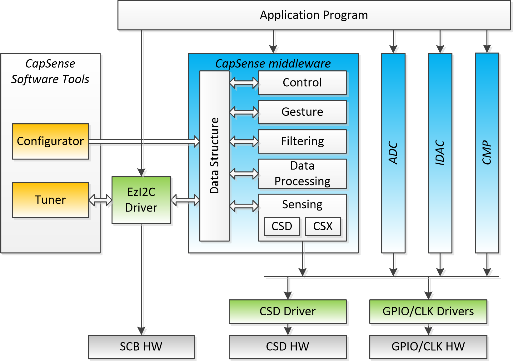
This section describes only the CSD driver. Refer to the corresponding sections for documentation of middleware supported by the CSD HW block.
The CSD driver is a low-level peripheral driver that provides an interface to a complex mixed signal of the CSD HW block.
The CSD driver alone does not provide system-level functions. Instead, it is used by upper-level middleware to configure the CSD HW block required by an application.
The CSD HW block can support only one function at a time. To allow seamless time-multiplex implementation of functionality and to avoid conflicting access to hardware from the upper level, the CSD driver also implements a lock semaphore mechanism.
The CSD driver supports re-entrance. If a device contains several CSD HW blocks, the same CSD driver is used to configure any HW block. For that, each function of the CSD driver contains a base address to define the CSD HW block to which the CSD driver communicates.
For dual-core devices, the CSD driver functions can be called either by the CM0+ or CM4 cores. In case both cores need access to the CSD Driver, you should properly manage the memory access.
There is no restriction on the CSD Driver usage in RTOS.
The CSD driver is simple wrapper driver specifically designed to be used by higher level middleware. Hence, is highly not recommended to use CSD driver directly in the application program. To incorporate CSD HW block functionality in the application program, an associated middleware should be used.
The CSD Driver can be used to implement a custom sensing solution. In such a case, the application program must acquire and lock the CSD HW block prior to accessing it.
Setting up and using the CSD driver can be summed up in these four stages:
The following code snippet demonstrates how to capture the CSD HW block for custom implementation:
The entire solution, either CapSense or CSDADC, in addition to the CSD HW block, incorporates the following instances:
The CSD driver does not configure those blocks and they should be managed by an upper level. When using CapSense or CSDADC, those blocks are managed by middleware.
The CSD HW block requires a peripheral clock (clk_peri) input. It can be assigned using two methods:
Any analog-capable GPIO pin that can be connected to an analog multiplexed bus (AMUXBUS) can be connected to the CSD HW block as an input.
GPIO input can be assigned to the CSD HW block using the following methods:
If middleware is used, pin configuration is managed by middleware. When using the CSD driver for custom implementation, the application program must manage pin connections.
Each AMUXBUS can be split into multiple segments. Ensure the CSD HW block and a GPIO belong to the same bus segment or join the segments to establish connection of the GPIO to the CSD HW block.
For more information about pin configuration, refer to the GPIO (General Purpose Input Output) driver.
The CSD HW block requires a reference voltage input to generate programmable reference voltage within the CSD HW block. There are two on-chip reference sources:
For more information about specification and startup of reference voltage sources, refer to the SysAnalog (System Analog Reference Block) driver prior to making the selection.
The CSD HW block has one interrupt that can be assigned to either the Cortex M4 or Cortex M0+ core. The CSD HW block can generate interrupts on the following events:
Additionally, the CSD interrupt can wake the device from the Sleep power mode. The CSD HW block is powered down in the Deep Sleep or Hibernate power modes. So, it cannot be used as a wake-up source in these power modes.
If a CapSense or ADC middleware is used, the interrupt service routine is managed by middleware. When using the CSD driver for custom implementation or other middleware, the application program must manage the interrupt service routine.
Implement an interrupt routine and assign it to the CSD interrupt. Use the pre-defined enumeration as the interrupt source of the CSD HW block. The CSD interrupt to the NVIC is raised any time the intersection (logic AND) of the interrupt flags and the corresponding interrupt masks are non-zero. The peripheral interrupt status register should be read in the ISR to detect which condition generated the interrupt. The appropriate interrupt registers should be cleared so that subsequent interrupts can be handled.
The following code snippet demonstrates how to implement a routine to handle the interrupt. The routine is called when a CSD interrupt is triggered.
The following code snippet demonstrates how to configure and enable the CSD interrupt:
For more information, refer to the SysInt (System Interrupt) driver.
Alternatively, instead of handling the interrupts, the Cy_CSD_GetConversionStatus() function allows for firmware polling of the CSD block status.
The CSD HW block can operate in Active and Sleep CPU power modes. It is also possible to switch between Low power and Ultra Low power system modes. In Deep Sleep and in Hibernate power modes, the CSD HW block is powered off. When the device wakes up from Deep Sleep, the CSD HW block resumes operation without the need for re-initialization. In the case of wake up from Hibernate power mode, the CSD HW block does not retain configuration and it requires re-initialization.
Refer to the SysPm (System Power Management) driver for more information about low-power mode transitions.
For more information, refer to the following documents:
| MISRA Rule | Rule Class (Required/Advisory) | Rule Description | Description of Deviation(s) |
|---|---|---|---|
| 14.2 | R | All non-null statements shall either: a) have at least one side-effect however executed, or b) cause control flow to change. | The unused function parameters are cast to void. This statement has no side effect and is used to suppress a compiler warning. |
| 20.6 | R | The macro offsetof, in library <stddef.h>, shall not be used. | The only CSD HW block register offsets are defined using this macro to implement functions Read/WriteReg. |
| Version | Changes | Reason for Change |
|---|---|---|
| 1.10.1 | Documentation updates | Update middleware references |
| 1.10 | The CSD driver sources are enclosed with the conditional compilation to ensure a successful compilation for non-CapSense-capable devices | Compilation for non-CapSense-capable devices |
| Changed the Cy_CSD_GetConversionStatus() function implementation | Fixed defect | |
| 1.0.1 | Documentation updates | Improve user's experience |
| 1.0 | The initial version |
API Reference | |
| Macros | |
| Functions | |
| Data Structures | |
| Enumerated Types | |