This driver provides API functions to configure the CT DAC subsystem of the Autonomous Analog.
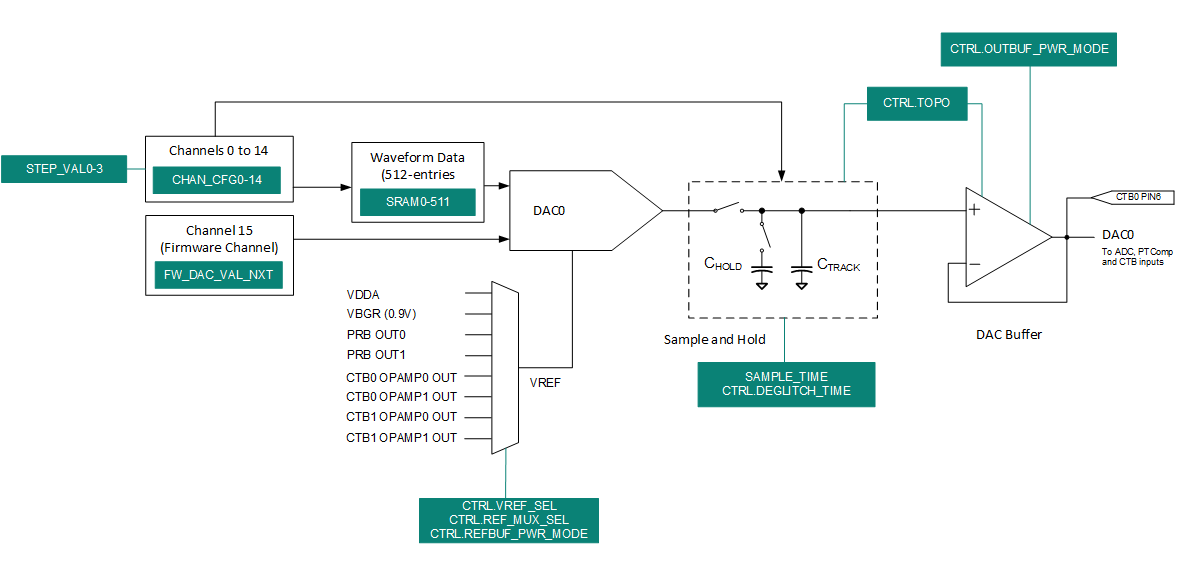
The CT DAC (hereafter DAC) is a 12-bit, continuous-time segmented DAC. It is based on an 8-bit R-2R array and a 4-bit thermometer array. A buffered sample and hold (S/H) circuit is useful for low power operation where an occasional update of the DAC output is acceptable. The DAC can be used in applications that require voltage references, bias, or analog waveform output. The DAC can work in conjunction with the CTB and PRB, which are used as buffered reference voltage sources.
For more information on the CT DAC, refer to the device Architecture Technical Reference Manual (TRM).
For the exact location of the pins, see the device datasheet.
Static Configuration
The static configuration contains application-specific settings intended to remain static for any DAC application. The Autonomous Controller (AC) will NOT change the static configuration during operation.
The static configuration of the DAC includes:
- Clock rate (for Low Power mode only);
- Input data format (signed/unsigned);
- Reference voltage source selector;
- DAC topology and use of reference and output voltage buffers;
- Output control settings;
For configuration settings, refer to cy_stc_autanalog_dac_sta_t.
DAC Channels and State Transition Table
Up to 15 configurations are available for the "virtual" DAC channels. The last channel with index 15 is preserved for updates from FW only.
The DAC channel configuration includes:
- Operating mode of the DAC (refer to Operating Mode chapter);
- The option to enable the S/H functionality (refer to Sample and Hold chapter)
- Start/end address and step size for the waveform in the LUT;
- Output voltage range;
For the configuration settings, refer to cy_stc_autanalog_dac_ch_t structure.
The DAC channel can be switched by the Autonomous Controller (AC) in runtime per settings provided in the State Transition Table (refer to cy_stc_autanalog_stt_dac_t structure)
Topology
Reference Voltage
The reference voltage can be Vdda or an internal Vref used with or without the unity gain buffer for the reference voltage in the DAC:
- VBGR - Internal, temperature-independent, band-gap voltage reference;
- CTB_OA - The reference voltage is driven by the Opamp output in the CTB (refer to CTB (Continuous Time Block) section);
- PRB_VREF - The reference voltage is driven from the PRB (refer to cy_stc_autanalog_prb_t structure);
- Note
- Vdda is 1.8V and Vbgr is 0.9V
Output Paths
The DAC output can be routed in different paths:
- Direct output path (NOT to pin);
- Direct output path with Ctrack capacitor connected;
- Direct output path with Ctrack and Chold capacitors connected;
- Buffered output path for internal connection within the chip;
- Buffered output path for internal and external connections;
Buffer Input and Output Ranges
The input range of the buffer can be rail-to-rail if the charge pump is enabled. Without the charge pump, the input range is 0 V to VDDA - 1.5 V. The output range of the buffer is typically 0.2 V to VDDA - 1.0 V and will depend on the load. See the device datasheet for more details.
| Charge Pump | Input Range | Output Range |
| Enabled | 0 V to VDDA | 0.2 V to VDDA - 0.2 V |
| Disabled | 0 V to VDDA - 1.5 V | 0.2 V to VDDA - 1.0 V |
- Note
- The charge pump nominal clock is 4MHz
For the configuration settings, see cy_en_autanalog_dac_out_buf_pwr_t.
Update Rates
The DAC supports two update rates of operation:
- Single step mode (default);
- Continuous mode;
In Single step mode, the DAC output changes on each subsequent trigger cy_stc_autanalog_stt_dac_t::trigger in the State Transition Table.
In Continuous mode, the output value changes on each subsequent clock of the DAC.
For more details, refer to Operating Mode.
Clocking
The DAC is clocked from the SRSS peripheral clock (Clk_HF9, up to 80MHz, refer to General Configuration Considerations) in chip Active mode using Peri 0 Clock Group 2 8-bit divider in the clock chain.
Or from the local Low Power Oscillator (LPOSC, 4096kHz, refer to cy_en_autanalog_timer_clk_src_t) in chip Deep Sleep mode.
The clock value can also be adjusted using the cy_stc_autanalog_dac_sta_t::lpDivDac, which divides the incoming clock in chip Deep Sleep mode.
Sample and Hold
The cy_stc_autanalog_dac_ch_t::sampleAndHold mode allows duty cycling of the DAC where Chold capacitor (Chold >> Ctrack) holds the previous value of the DAC output. The cy_stc_autanalog_dac_sta_t::sampleTime is defined as the time it takes for the DAC output to drop by 1 LSB.
The DAC is updated every positive edge of the DAC clock with the following sequence:
- The DAC is configured for SAMPLE: the COS and CHD switches are closed, DAC array is enabled and outputs the updated value (based on Operating Mode) onto a Chold capacitor for sample time duration;
- The DAC is configured for HOLD: the COS switch is opened, CHD switch is closed, DAC array is disabled and the last output value is held on the Chold capacitor until the next positive edge of the DAC clock. HOLD duration is DAC clock period - duration of the sample time.
- Note
- For Operating Mode ADDRESS or DATA, the AC must wait (ACTION = WAIT_FOR) for the DAC strobe (CONDITION = DAC_STROBE) before re-triggering the DAC_INC/DAC_DEC fields. Refer to cy_en_autanalog_stt_ac_action_t and cy_en_autanalog_stt_ac_condition_t.
De-glitch
A typical issue in DACs is the glitch during code transitions. Blanking can be used to reduce the glitch. During data changes, a dedicated switch on the output path is used to block the glitch from propagating to the DAC output. The Ctrack capacitor maintains the previous value while the switch is open, so the DAC output doesn't drop.
If cy_stc_autanalog_dac_sta_t::topology is set to
- CY_AUTANALOG_DAC_TOPO_DIRECT;
- CY_AUTANALOG_DAC_TOPO_DIRECT_WITH_TRACK_CAP;
- CY_AUTANALOG_DAC_TOPO_DIRECT_WITH_TRACK_HOLD_CAP;
the CHD switch is opened during the de-glitch time.
If cy_stc_autanalog_dac_sta_t::topology is set to
- CY_AUTANALOG_DAC_TOPO_BUFFERED_INTERNAL;
- CY_AUTANALOG_DAC_TOPO_BUFFERED_EXTERNAL;
the COS switch is opened during the de-glitch time.
De-glitch time set with cy_stc_autanalog_dac_sta_t::deGlitchTime and calculated as follow:
(DEGLITCH_CNT + 1) / DAC_CLOCK_FREQ
Operating Mode
| Mode | Description |
| One Shot, One Quadrant | The LUT address is incremented on every positive edge of the DAC clock until the END_ADDR is reached or exceeded.
The update step size is defined by STEP_VAL.
The One Shot mode is completed when the END_ADDR is reached.
The DAC outputs an EPOCH trigger after reaching (or exceeding) the END_ADDR and outputting the corresponding value. |
| One Shot, Two Quadrant | The LUT address is incremented on every positive edge of the DAC clock until the END_ADDR is reached*, then the LUT address is decremented back to the START_ADDR.
The DAC outputs an EPOCH trigger after returning to (or exceeding) the START_ADDR and outputting the corresponding value. - Note
- *If the END_ADDR is not reached but exceeded (which can happen with STEP_VAL greater than 1), the LUT address is decremented from the END_ADDR by the amount exceeded).
After outputting the END_ADDR in one direction, while wrapping around in the reverse direction, the STEP_VAL is decremented from this last address value (i.e. we output the last value only once and while wrapping around in the reverse direction, we output the address that is the last address minus the STEP_VAL).
|
| One Shot, Four Quadrant | The LUT address is updated on every positive edge of the DAC clock according to the following algorithm:
- The LUT address is incremented until the END_ADDR is reached*
- The LUT address is decremented until the START_ADDR is reached*
- The polarity of the DAC output signal is inverted and steps 1 and 2 are repeated
The DAC outputs an EPOCH trigger after returning to (or exceeding) the START_ADDR with an inverted polarity and outputting the corresponding value.
This mode assumes that the DAC waveform table constitutes 1/4 of the desired generated waveform. - Note
- *If the START_ADDR/END_ADDR address is not reached but instead exceeded (which can happen with STEP_VAL greater than 1), the LUT address is adjusted (i.e. decremented from END_ADDR or incremented from START_ADDR by the amount exceeded).
After outputting the START/END ADDR in one direction, while wrapping around in the opposite direction, the STEP_VAL is incremented/decremented from this last address value (i.e. we output the last value only once and when we go back in the opposite direction, we output the address that is the last address plus/minus the STEP_VAL).
|
| Continuous, One Quadrant | The LUT address is incremented on every positive edge of the DAC clock until the END_ADDR is reached*.
The address then wraps back to the START_ADDR and repeats indefinitely.
The update step size is defined by STEP_VAL.
The DAC outputs an EPOCH trigger after reaching (or exceeding) the END_ADDR and outputting the corresponding value. - Note
- *If the END_ADDR is not reached, but instead exceeded (which can happen with STEP_VAL greater than 1), the LUT address wraps back to START_ADDR and is incremented by the amount exceeded).
|
| Continuous, Two Quadrant | The LUT address is incremented on every positive edge of the DAC clock until the END_ADDR is reached*, then the LUT address is decremented back to the START_ADDR and repeats indefinitely.
The DAC outputs an EPOCH trigger after returning to the START_ADDR and outputting the corresponding value. - Note
- *If the START_ADDR or the END_ADDR is not reached but instead exceeded (which can happen with STEP_VAL greater than 1), the LUT address is adjusted (i.e. decremented from END_ADDR or incremented from START_ADDR by the amount exceeded).
After outputting the START/END ADDR in one direction, while wrapping around in the opposite direction, the STEP_VAL is incremented/decremented from this last address value (i.e. we output the last value only once and while wrapping around we output the address which is the last address plus/minus the STEP_VAL).
|
| Continuous, Four Quadrant | The LUT address is updated on every positive edge of the DAC clock according to the following algorithm:
- The LUT address is incremented until the END_ADDR is reached*.
- The LUT address is decremented until the START_ADDR is reached*.
- The polarity of the DAC output signal is inverted and steps 1 and 2 are repeated indefinitely.
The DAC outputs an EPOCH trigger after returning to (or exceeding) the START_ADDR with an inverted polarity and outputting the corresponding value.
This mode assumes that the DAC waveform table constitutes 1/4 of the desired generated waveform. - Note
- *If the START_ADDR/END_ADDR is not reached but instead exceeded (which can happen with STEP_VAL greater than 1), the LUT address is adjusted (i.e. decremented from END_ADDR or incremented from STAR_ADDR by the amount exceeded).
After outputting the START/END ADDR in one direction, while wrapping around in the opposite direction, the STEP_VAL is incremented/decremented from this last address value (i.e. we output the last value only once and while wrapping around in the opposite direction, we output the address that is the last address plus/minus the STEP_VAL).
|
| Address mode | The LUT address is updated on every positive edge of the DAC_INC or DAC_DEC from the State Transition Table, see cy_stc_autanalog_stt_dac_t::direction, unless cy_stc_autanalog_dac_ch_t::sampleAndHold is set
(for more details, refer to Sample and Hold chapter).
The update step size is defined by STEP_VAL.
If on the START_ADDR and DAC_DEC is triggered, the address wraps forward to the END_ADDR.
If on the END_ADDR and DAC_INC is triggered, the address wraps back to the START_ADDR.
- Note
- In this mode, the DAC does not output an EPOCH trigger.
-
The DAC does not support validation range conditions for address, see cy_stc_autanalog_dac_ch_limit_t
|
| Data mode | The DAC outputs the data stored at the START_ADDR.
The DAC output value is incremented or decremented based on every positive edge of the DAC_INC or DAC_DEC from the State Transition Table, see cy_stc_autanalog_stt_dac_t::direction, unless cy_stc_autanalog_dac_ch_t::sampleAndHold is set
(for more details, refer to Sample and Hold chapter).
The increment/decrement amount is set by STEP_VAL.
- Note
- In this mode, the DAC does not output an EPOCH trigger.
-
The DAC value is clamped if requested to go under the minimum code (0x000 for unsigned or 0x800 for signed) or above the maximum code (0xFFF for unsigned or 0x7FF for signed).
|
Where START_ADDR, END_ADDR and STEP_VAL are configured individually for each channel:
Output Drive Control
The DAC can be programmed so that code 0 corresponds to ground or 1 LSB. The bottom end of the R-2R ladder (LSB side) can be configured to connect to the Vref or Vssa using cy_stc_autanalog_dac_sta_t::bottomSel. This setting determines the output drive control in row with cy_stc_autanalog_stt_dac_t::enable, cy_stc_autanalog_dac_waveform_t::driveMode and cy_stc_autanalog_dac_sta_t::disabledMode as follow:
| DAC Enabled | Drive Mode | Disabled Mode | DAC Range | Output State |
| FALSE | X | X | X | tri-state |
| TRUE | Hi-Z | tri-state | X | tri-state |
| TRUE | Hi-Z | Vssa/Vref | Vssa | Vssa |
| TRUE | Hi-Z | Vssa/Vref | Vref | Vref |
| TRUE | Vref | tri-state | X | tri-state |
| TRUE | Vref | Vssa/Vref | Vssa | Vssa |
| TRUE | Vref | Vssa/Vref | Vref | Vref |
| TRUE | Enabled | X | Vssa | [0, 4095] * Vref / 4096 |
| TRUE | Enabled | X | Vref | [1, 4096] * Vref / 4096 |
Signed/Unsigned Input
The format of the DAC code can be either unsigned or signed two's complement. Only the first 12 bits are used by the DAC, so no sign extension is required. For the signed format, the DAC decodes the input code by adding 0x800.
For the configuration settings, see cy_stc_autanalog_dac_sta_t::sign.
Interrupts, Triggers and STT Events
The following internal events of the DAC can be configured to generate an interrupt or trigger or used as the STT event in the Autonomous Analog (refer to cy_en_autanalog_ac_out_trigger_mask_t and cy_en_autanalog_stt_ac_condition_t):
- DAC_EPOCH - Indicates end of waveform event;
- DAC_RANGE - Indicates range detection conditions;
- DAC_EMPTY (interrupt only) - Indicates empty conditions on FW channel (Ch#15), refer to Cy_AutAnalog_DAC_WriteNextSample ;
- DAC_STROBE (STT event only) - Indicates the S/H iteration finished (refer to Sample and Hold chapter);
Sample use case: FW Channel #15
#define DAC0IDX (0U)
#define DAC1IDX (1U)
{
.low = 0x638,
.high = 0x640,
};
{
.deGlitch = false,
.bottomSel = false,
.disabledMode = true,
.sign = false,
.sampleTime = 0U,
.stepVal = {0U, 0U, 0U},
.deGlitchTime = 0U,
.chCfg = {NULL},
.chLimitCfg = {&dac0Ch15StatusCfg, NULL, NULL},
};
{
.waveform = NULL,
};
{
{
.enable = true,
.trigger = false,
.channel = 15U,
},
};
cy_en_autanalog_dac_limit_t cond
Range detection condition.
Definition: cy_autanalog_dac.h:872
bool unlock
DAC Unlock .
Definition: cy_autanalog_dac.h:1018
cy_stc_autanalog_dac_sta_t * dacStaCfg
The pointer to a static part of the DAC configuration.
Definition: cy_autanalog_dac.h:1004
uint16_t lpDivDac
The Low Power clock divider, actual divide value is DIV_VAL + 1, valid range is 1....
Definition: cy_autanalog_dac.h:900
The channel range detection configuration structure.
Definition: cy_autanalog_dac.h:871
Defines the static configuration structure, see Static Configuration.
Definition: cy_autanalog_dac.h:899
The configuration structure to set up the entire DAC.
Definition: cy_autanalog_dac.h:1002
The DAC section in the State Transition Table state.
Definition: cy_autanalog_dac.h:1017
@ CY_AUTANALOG_DAC_VREF_MUX_VBGR
The DAC reference is VBGR.
Definition: cy_autanalog_dac.h:709
@ CY_AUTANALOG_DAC_REF_BUF_PWR_OFF
The power mode for the buffer is OFF, the buffer is disabled.
Definition: cy_autanalog_dac.h:605
@ CY_AUTANALOG_DAC_CH_LIMIT_OUTSIDE
The DAC value must satisfy the following: (Value < cy_stc_autanalog_dac_ch_limit_t::low) OR (Value >...
Definition: cy_autanalog_dac.h:809
@ CY_AUTANALOG_DAC_DIRECTION_FORWARD
Forward/Increment.
Definition: cy_autanalog_dac.h:823
@ CY_AUTANALOG_DAC_OUT_BUF_PWR_ULTRA_LOW
The power mode for the buffer is ULTRA LOW, the charge pump is OFF, the buffer quiescent current is...
Definition: cy_autanalog_dac.h:652
@ CY_AUTANALOG_DAC_VREF_VDDA
The DAC reference is driven directly from the Vdda.
Definition: cy_autanalog_dac.h:590
@ CY_AUTANALOG_DAC_TOPO_BUFFERED_EXTERNAL
The output of the DAC is buffered for internal or external connections.
Definition: cy_autanalog_dac.h:575
cy_en_autanalog_status_t
Return the status for functions of the Autonomous Analog driver.
Definition: cy_autanalog_common.h:109
{
}
cy_en_autanalog_status_t Cy_AutAnalog_DAC_LoadConfig(uint8_t dacIdx, const cy_stc_autanalog_dac_t *dacCfg)
Configures the DAC per provided static and waveform settings.
Definition: cy_autanalog_dac.c:50
__STATIC_INLINE void Cy_AutAnalog_DAC_WriteNextSample(uint8_t dacIdx, int32_t sample)
Loads a value that will update the DAC output on the next refresh cycle, applicable to FW channel #15...
Definition: cy_autanalog_dac.h:1181
@ CY_AUTANALOG_SUCCESS
Initialization completed successfully.
Definition: cy_autanalog_common.h:110
Sample use case: Output Analog Waveform
#define DAC0IDX (0U)
#define DAC1IDX (1U)
#define WAVEFORM_CH_IDX (0U)
#define WAVEFORM_SUMPLES_NUM (6U)
#define WAVEFORM_START_IDX (0U)
#define WAVEFORM_END_IDX (5U)
static int16_t waveform[WAVEFORM_SUMPLES_NUM] =
{
0x0BFFU,
0x0BFFU,
0x0BFFU,
0x0FFFU,
0x0FFFU,
0x0FFFU,
};
{
};
{
.waveformData = waveform,
.isDriveModeArray = true,
.driveMode = driveModeArr,
};
{
.endAddr = WAVEFORM_END_IDX,
.sampleAndHold = false,
};
{
.deGlitch = true,
.bottomSel = false,
.disabledMode = true,
.sign = false,
.sampleTime = 0U,
.stepVal = {0U, 0U, 0U},
.deGlitchTime = 2U,
.chCfg = {&dac1Ch0Cfg, },
.chLimitCfg = {NULL},
};
{
.waveform = &dac1Waveform,
};
{
{
.enable = true,
.trigger = true,
.channel = WAVEFORM_CH_IDX,
},
};
uint16_t startAddr
Start address of the waveform in the LUT.
Definition: cy_autanalog_dac.h:845
uint16_t numSamples
The number of samples in the waveform.
Definition: cy_autanalog_dac.h:885
The configuration structure of the DAC channel.
Definition: cy_autanalog_dac.h:844
cy_en_autanalog_dac_out_drive_mode_t
Defines the drive mode for the DAC output, for more details, refer to the device Architecture Technic...
Definition: cy_autanalog_dac.h:786
@ CY_AUTANALOG_DAC_VREF_MUX_PRB_OUT0
The DAC reference is Vref0 from the PRB0.
Definition: cy_autanalog_dac.h:714
@ CY_AUTANALOG_DAC_REF_BUF_PWR_ULTRA_LOW_RAIL
The power mode for the buffer is ULTRA LOW, the charge pump is ON, the buffer quiescent current is ...
Definition: cy_autanalog_dac.h:611
@ CY_AUTANALOG_DAC_LUT_CONT_FOUR_QUAD
The LUT mode is Continuous Four Quadrant.
Definition: cy_autanalog_dac.h:731
@ CY_AUTANALOG_DAC_STEP_SEL_DISABLED
The selector is not used, the step value is 1 by default.
Definition: cy_autanalog_dac.h:745
@ CY_AUTANALOG_DAC_STATUS_SEL_DISABLED
The selector is not used, the DAC output is not validated for compliance with the range conditions.
Definition: cy_autanalog_dac.h:766
@ CY_AUTANALOG_DAC_OUT_DRIVE_MODE_EN
The DAC output is enabled (outputs appropriate value)
Definition: cy_autanalog_dac.h:787
@ CY_AUTANALOG_DAC_VREF_MUX_OUT
The DAC reference is driven by the reference multiplexer, see cy_en_autanalog_dac_vref_mux_t.
Definition: cy_autanalog_dac.h:586