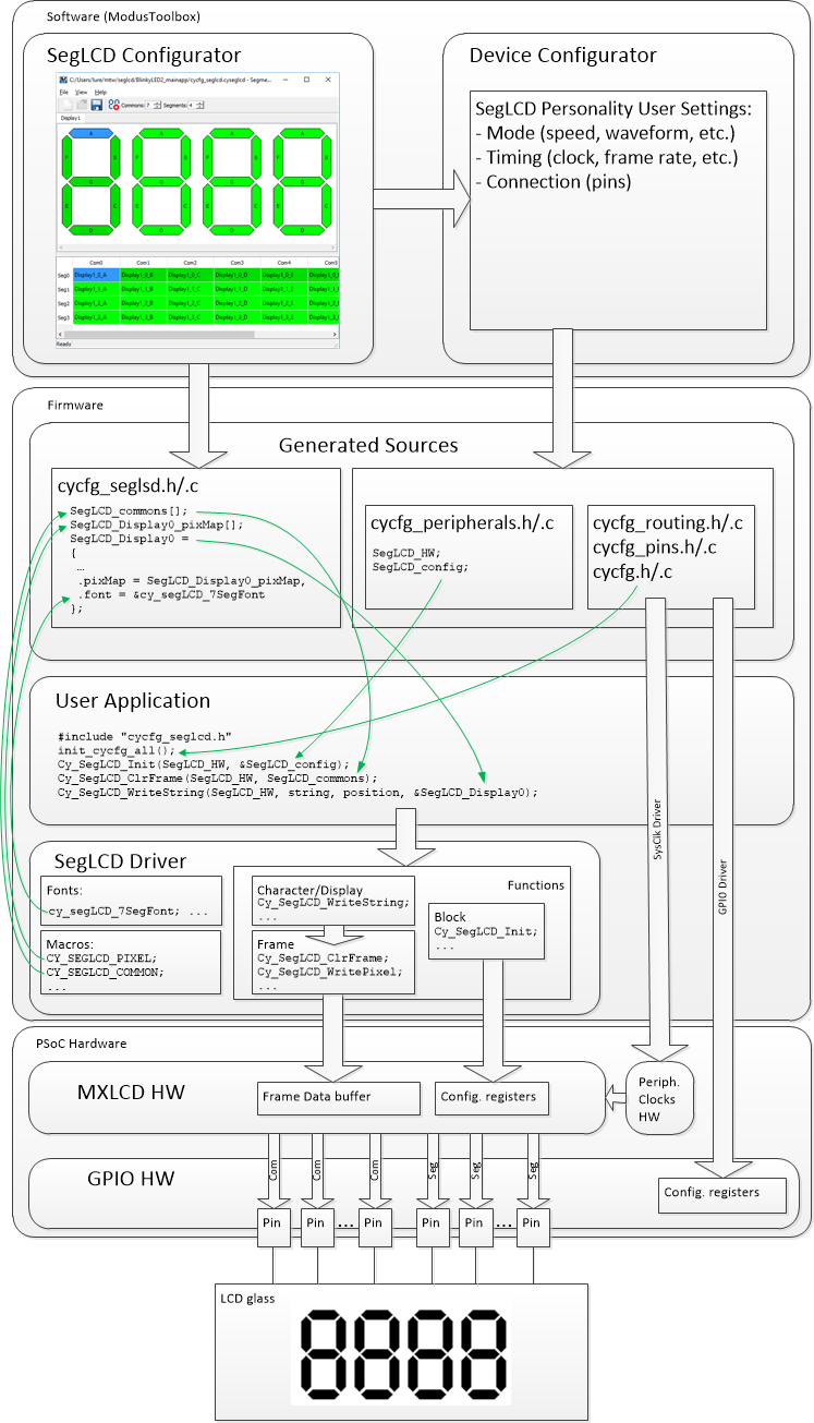
The Segment LCD Driver provides an API to configure and operate the MXLCD hardware block.
The MXLCD block can be flexibly configured to drive a variety of LCD glass at different voltage levels with multiplex ratios.
Features:
- Digital Correlation and PWM at 1/2, 1/3, 1/4 and at 1/5 bias modes are supported
- Drives STN/TN LCD-glass with up to eight COMs (device specific)
- 30 to 150 Hz refresh rate
- Supports both type A (standard) and type B (low-power) waveforms
- The display pixel state can be inverted for a negative image
- Operation in Deep Sleep Mode from ILO/MFO
- All-digital contrast control using "Dead Period" digital modulation
- A set of basic standard displays and fonts
- The customizable display and font structures.
Glossary
- LCD - Liquid Crystal Display
- Glass - An LCD glass with one or more displays (e.g. one 7-segment display and one bar-graph display).
- TN - A twisted nematic LCD glass.
- STN - A super-twisted nematic LCD glass.
- Display - A block of the same type of symbols on an LCD glass to indicate a multi-digital number or character string. There may be one or more displays on a single LCD glass.
- Symbol - A block of pixels on an LCD glass to indicate a single digit or character.
- Pixel - A basic displaying item. This can be a segment of a 7-segment symbol (thus called a "segment"), a pixel of a dot-matrix display, or a stand-alone arbitrarily-shaped display element. Each pixel has a unique set of common and segment lines within one LCD glass. The API offers pixel identifiers - the 32-bit items of the display pixel map (to use in the display structure definition, see cy_stc_seglcd_disp_t), created by the CY_SEGLCD_PIXEL macro.
- Common line (Com/COM for short) - A common wire/signal from the PSoC chip to the LCD glass. The API offers common line identifiers - the 32-bit items of the commons array (to use in Cy_SegLCD_ClrFrame and Cy_SegLCD_InvFrame), created by the CY_SEGLCD_COMMON macro.
- Segment line (Seg/SEG for short) - A segment wire/signal from the PSoC chip to the LCD glass.
- Octet - A bunch of subsequent eight MXLCD terminals. Octets may not match GPIO ports.
- Frame buffer - An array of registers to control the MXLCD signal generation for all the MXLCD terminals.
SegLCD Solution
The Segment LCD Driver can be used either as a standalone library to manage the MXLCD hardware or as a part of the more complex software solution delivered within ModusToolbox: the Device Configurator SegLCD personality and the SegLCD Configurator tools.
The SegLCD solution provides an easy method to configure an MXLCD block to drive your standard or custom LCD glass:
The SegLCD solution includes:
- The SegLCD Configurator tool, which is a display configuration wizard to create and configure displays and generate commons array and display structures cy_stc_seglcd_disp_t.
- The ModusToolbox Device Configurator contains a SegLCD personality, which is an MXLCD block configuration wizard. It helps to easily tune all the timing settings, operation modes, provides a flexible GPIO pin assignment capability and generates the cy_stc_seglcd_config_t structure and the rest of accompanying definitions.
- The SegLCD Driver API itself, which uses all the mentioned above generated code.
Configuration Considerations
To start working with an LCD, first initialize the MXLCD block, then initialize the frame buffer, and then enable the block:
{
.comNum = 8,
.frRate = 70,
.contrast = 70,
};
const uint32_t commons[8] =
{
};
- Note
- If you use ModusToolbox Device Configurator, a SegLCD configuration structure is generated automatically into the GeneratedSource/cycfg_peripherals.h/.c files. All you need is just to call Cy_SegLCD_Init with a pointer to the structure.
{
{
}
else
{
}
}
else
{
}
Contrast vs. Frame Rate (cy_stc_seglcd_config_t::contrast vs. cy_stc_seglcd_config_t::frRate)
Some combinations of a frame rate and input frequency can restrict the valid contrast range because of the limited dividers size (for Low Speed mode - 8 bit, and for High Speed mode - 16 bit). For small values of contrast at small frame rates, the required divider values may be beyond permissible limits of the dividers size. For large High Speed clock frequencies, certain ratios between the contrast and frame rate cannot be achieved due to the limited divider size. The Cy_SegLCD_Init function automatically restricts such incorrect combinations (returns CY_SEGLCD_BAD_PARAM). The peripheral clock divider can be adjusted to clock the LCD block with proper clock frequency:
Speed Mode Switching (cy_stc_seglcd_config_t::speed)
The High Speed and Low Speed generators mostly duplicate each other, except that for MXLCD_ver1, the High Speed version has larger frequency dividers to generate the frame and sub-frame periods. This is because the clock of the High Speed block typically has a frequency 30-100 times bigger than the 32 KHz clock fed to the Low Speed block. For MXLCD_ver2, both High Speed and Low Speed generators have similar 16-bit dividers, because a possibility exists to source a Low Speed generator with a Medium Frequency clock (see Medium Frequency Domain Clock) that may be much higher than 32 KHz ILO:
Switching between High Speed and Low Speed modes via the Cy_SegLCD_Init function causes the dividers to reconfigure. Under possible restrictions related to certain ratios between contrast and frame rates (see Contrast vs. Frame Rate section above), switching between High Speed and the Low Speed modes via the Cy_SegLCD_Init function may set new dividers values that don't give the same contrast value.
Driving Modes (cy_stc_seglcd_config_t::drive)
SegLCD supports the following operating modes:
- Digital Correlation - preferred for low clock speeds, low common lines count and low supply voltages.
- PWM at 1/2, 1/3, 1/4 or 1/5 Bias - preferred for high clock speeds (e.g. over 1MHz), many common lines (e.g. over 4), and high voltages (e.g. 3.3V or higher). More precise preferences depend on a certain set of an LCD glass, power modes, the number of terminals, desired contrast/frame rate settings, etc.
Conventional Waveforms (cy_stc_seglcd_config_t::wave)
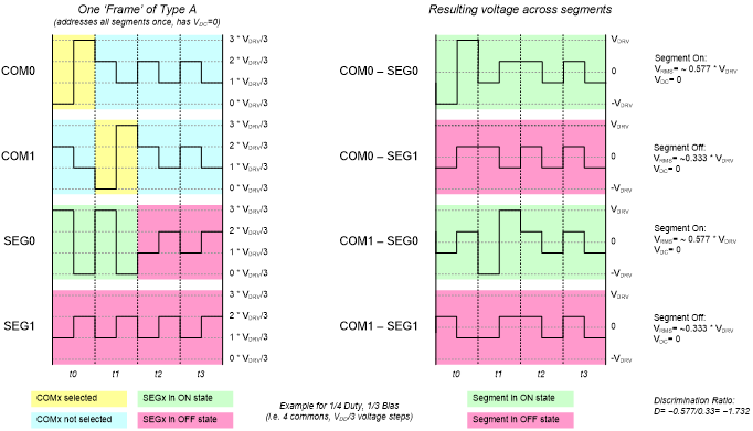
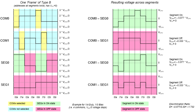
Conventional LCD drivers apply waveforms to COM and SEG electrodes generated by switching between multiple different voltages. The following terms are used to define these waveforms:
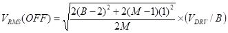
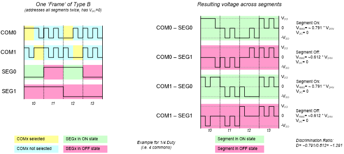
- Duty: A driver operates in the 1/M-th duty when it drives M COM electrodes. Each COM electrode is effectively driven for the 1/M of the frame time.
- Bias: A driver uses the 1/B-th bias when its waveforms use the voltage steps of (1/B)*VDRV.
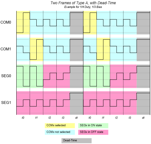
- Frame: A frame is the time length to address all segments. During a frame, the driver cycles through the commons in sequence. All segments receive 0V DC when measured over the length of an entire frame.
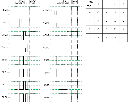
- Type-A Waveform: The driver structures the frame into M sub-frames. COMi is addressed in sub-frame i.
- Type-B Waveform: The driver structures the frame into 2M sub-frames. COMi is addressed in sub-frames i and M+i. The two sub-frames are inverse of each other. Typically, type-B waveforms are slightly more power-efficient because they contain fewer transitions.
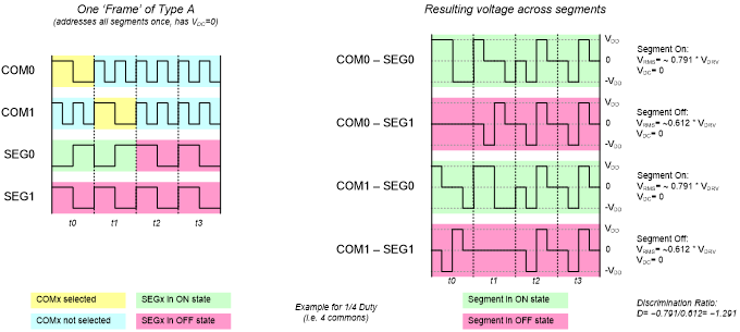
The following figures show the conventional waveforms for COM and SEG electrodes for the 1/3rd bias and 1/4th duty. Only COM0/COM1 and SEG0/SEG1 are drawn. Conventional Type-A Waveform Example:
Conventional Type-B Waveform Example:
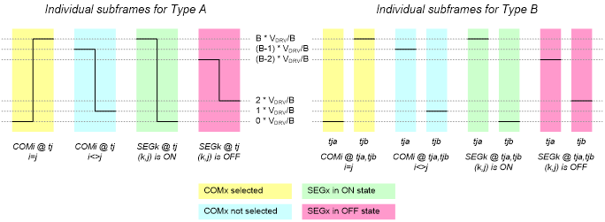
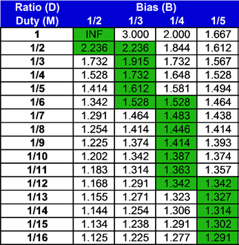
The generalized waveforms for individual sub-frames for any duty and bias are illustrated in the following figure. Note that these use 6 different voltages at most(including VSS and VDRV). Conventional Waveforms - Generalized:
The effective RMS voltage for on and off segments can be calculated using these waveforms:
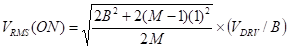
The resulting Discrimination Ratio (D) for various bias and duty combinations is illustrated in the following table. The bias choice (B) for each duty (M) with the highest possible value for D is colored green:
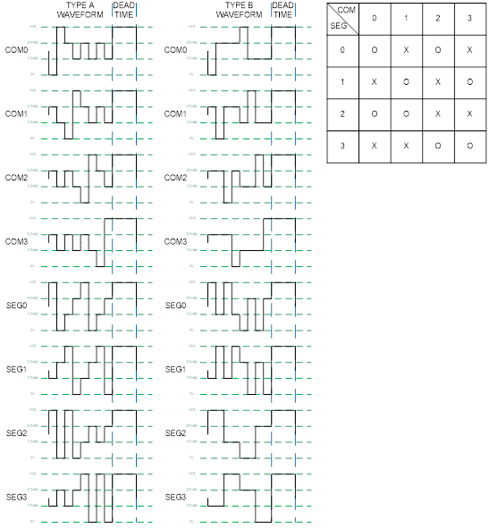
Digital Correlation (CY_SEGLCD_CORRELATION)
The principles of operation are illustrated by the example waveforms shown in the following figures. Digital Correlation Example - Type-A:
Digital Correlation Example - Type-B:
As illustrated, instead of generating bias voltages between the rails, this approach takes advantage of the LCD displays characteristic: the LCD segments' on-ness and off-ness degree is determined by the RMS voltage across the segments. In this approach, the correlation coefficient between any given pair of COM and SEG signals determines whether the corresponding LCD segment is On or Off. Thus, by doubling the base drive frequency of the COM signals in their inactive sub-frame intervals, the phase relationship of the COM and SEG drive signals can be varied to turn segments on and off - rather than varying the DC levels of the signals as is used in the conventional approaches.
PWM Drive (CY_SEGLCD_PWM)
This approach duplicates the multi-voltage drive signals of the conventional method with bias B using a PWM output signal together with the intrinsic resistance and capacitance of the LCD display to create a simple PWM DAC. This is illustrated in the following figure:
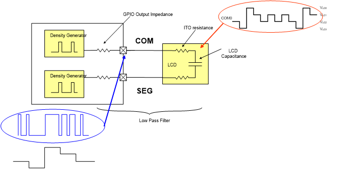
To drive a low-capacitance display with an acceptable ripple and rise/fall time, using a 32-kHz PWM an additional external series resistance of 100 k - 1 M ohm is required. External Resistors are not required for PWM frequencies of greater than ~1 MHz. The exact frequency depends on the display capacitance, the internal ITO resistance of the ITO routing traces, and the drive impedance of the I/O pins. The PWM method works for any bias value (B). NOTE As B gets higher, a higher PWM step frequency is required to maintain the same PWM output frequency (the RC response of the LCD depends on the PWM output frequency, NOT the step frequency). The PWM approach may also be used to drive a 1/2-bias display. This has the advantage that PWM is only required on the COM signals, as SEG signals of a 1/2-bias display use only logic levels. Therefore, PWM 1/2-bias can be supported at 32 kHz using just four external resistors. The power consumption of the approach (even for 1/2 bias) is substantially higher than that of other methods. Therefore, it is recommended power-sensitive customers use Digital Correlation drive in Deep Sleep mode, and change to PWM mode to gain the advantage of better contrast/viewing angle on TN displays in Active or Sleep mode.
PWM1/2 LCD drive waveform:
PWM1/3 LCD drive waveform:
Digital Contrast Control
In all modes, digital contrast control is available using the duty cycle/dead time method illustrated in the following figure:
This illustration shows the principle for 1/3 bias and 1/4 duty implementation, but the general approach of reducing contrast by reducing the percentage of time the glass is driven can be generalized and applied to any drive method. In all cases, during the dead time, all COM and SEG signals are set to a logic "1" state.
When the block is configured, for further work with display, a display structure is needed:
{
{
},
{
},
{
},
{
}
};
{
.symNum = 4,
.invert = false,
.pixMap = (uint32_t*)displayPixMap,
};
- Note
- Using the SegLCD Configurator, display structures and the commons array are generated automatically into the GeneratedSource/cycfg_seglcd.h/.c files. All you need is just to include cycfg_seglcd.h into your application code.
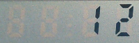
And now you can write multi-digit decimal and hexadecimal numbers and strings onto the initiated 7-segment display:
after which the next image on the glass appears:
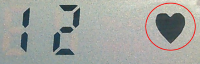
Or even manage separate LCD pixels:
#define HEART (CY_SEGLCD_PIXEL(LCD_P11_6, 7UL))
after which the next image on the glass appears:
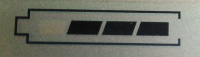
The basic use case of the bar-graph display type:
#define FRAME (CY_SEGLCD_PIXEL(LCD_P12_6, 7UL))
const uint32_t barGraphPixMap[BAR_LENGTH] =
{
};
{
.symNum = BAR_LENGTH,
.invert = false,
.pixMap = (uint32_t*)barGraphPixMap,
.font = NULL
};
uint32_t barGraphValue = 3UL;
after which the next image on the glass appears:
Also, you can customize basic fonts, for example:
const uint8_t customAsciiFontMap7Seg[] =
{
0x00U,0x00U,0x00U,0x00U,0x00U,0x00U,0x00U,0x00U,0x00U,0x00U,0x00U,0x00U,0x00U,0x40U,0x00U,0x00U,
0x3FU,0x06U,0x5BU,0x4FU,0x66U,0x6DU,0x7DU,0x07U,0x7FU,0x6FU,0x00U,0x00U,0x00U,0x00U,0x00U,0x00U,
0x00U,0x77U,0x7CU,0x39U,0x1FU,0x79U,0x71U,0x3DU,0x76U,0x06U,0x1EU,0x75U,0x38U,0x15U,0x37U,0x3FU,
0x73U,0x67U,0x33U,0x6DU,0x07U,0x3EU,0x72U,0x2AU,0x64U,0x66U,0x5BU,0x00U,0x00U,0x00U,0x00U,0x00U,
0x00U,0x5FU,0x7CU,0x58U,0x5EU,0x7BU,0x71U,0x6FU,0x74U,0x04U,0x0EU,0x7AU,0x38U,0x15U,0x54U,0x5CU,
0x73U,0x67U,0x50U,0x6DU,0x78U,0x1CU,0x62U,0x2AU,0x52U,0x6EU,0x5BU
};
{
.last = 'z',
.ascii = true,
.fontMap = customAsciiFontMap7Seg
};
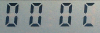
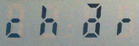
And now you can write characters and strings on a standard 7-segment display:
display.
font = &customAsciiFont7Seg;
after which the next image on the glass appears:
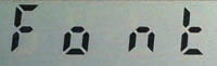
display.
font = &customAsciiFont7Seg;
{
}
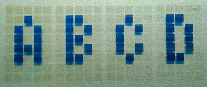
Also, you can customize or create your own displays, for example:
#define CUSTOM_DISP_3x5DM_TYPE (3 * 5)
const uint32_t commonsDm[] =
{
};
const uint32_t display3x5PixMap[4][CUSTOM_DISP_3x5DM_TYPE] =
{
{
},
{
},
{
},
{
}
};
{
.
type = CUSTOM_DISP_3x5DM_TYPE,
.symNum = 4,
.invert = false,
.pixMap = (uint32_t*)display3x5PixMap,
.font = &customNumericFont3x5
};
And also different fonts for them:
#define CUSTOM_DISP_3x5DM_FONT_SYM_SIZE (CY_SYSLIB_DIV_ROUNDUP(CUSTOM_DISP_3x5DM_TYPE, CY_SEGLCD_OCTET))
const uint8_t customNumericFontMap3x5[][CUSTOM_DISP_3x5DM_FONT_SYM_SIZE] =
{
{0x2EU,0x3AU},{0xF2U,0x43U},{0xB9U,0x4AU},{0xB1U,0x2AU},{0x87U,0x7CU},{0xB7U,0x26U},{0xAEU,0x26U},{0xA1U,0x0FU},
{0xAAU,0x2AU},{0xB2U,0x3AU},{0x3EU,0x79U},{0xBFU,0x2AU},{0x2EU,0x2AU},{0x3FU,0x3AU},{0xBFU,0x46U},{0xBFU,0x04U},{0x00U,0x00U}
};
{
.ascii = false,
.fontMap = (uint8_t*)customNumericFontMap3x5
};
const uint8_t customAsciiFontMap3x5[][CUSTOM_DISP_3x5DM_FONT_SYM_SIZE] =
{
{0x00U,0x00U},{0x00U,0x00U},{0x00U,0x00U},{0x00U,0x00U},{0x00U,0x00U},{0x00U,0x00U},{0x00U,0x00U},{0x00U,0x00U},
{0x00U,0x00U},{0x00U,0x00U},{0x00U,0x00U},{0x00U,0x00U},{0x00U,0x00U},{0x00U,0x00U},{0x00U,0x00U},{0x00U,0x00U},
{0x2EU,0x3AU},{0xF2U,0x43U},{0xB9U,0x4AU},{0xB1U,0x2AU},{0x87U,0x7CU},{0xB7U,0x26U},{0xAEU,0x26U},{0xA1U,0x0FU},
{0xAAU,0x2AU},{0xB2U,0x3AU},{0x00U,0x00U},{0x00U,0x00U},{0x00U,0x00U},{0x00U,0x00U},{0x00U,0x00U},{0x00U,0x00U},
{0x00U,0x00U},{0x3EU,0x79U},{0xBFU,0x2AU},{0x2EU,0x2AU},{0x3FU,0x3AU},{0xBFU,0x46U},{0xBFU,0x04U}
};
{
.last = 'F',
.ascii = true,
.fontMap = (uint8_t*)customAsciiFontMap3x5
};
And now use all that together:
There are LCD-GPIO terminal mapping definitions for different device families used in the mentioned above commons and display pixel arrays:
#if defined P13_0_PORT
#define LCD_P10_3 11UL
#define LCD_P10_4 12UL
#define LCD_P10_7 15UL
#define LCD_P11_0 16UL
#define LCD_P11_1 17UL
#define LCD_P11_2 18UL
#define LCD_P11_3 19UL
#define LCD_P11_4 20UL
#define LCD_P11_5 21UL
#define LCD_P11_6 22UL
#define LCD_P12_0 23UL
#define LCD_P12_1 24UL
#define LCD_P12_2 25UL
#define LCD_P12_3 26UL
#define LCD_P12_4 27UL
#define LCD_P12_5 28UL
#define LCD_P12_6 29UL
#define LCD_P12_7 30UL
#define LCD_P13_0 31UL
#define LCD_P13_1 32UL
#define LCD_P13_2 33UL
#define LCD_P13_3 34UL
#define LCD_P13_4 35UL
#define LCD_P13_5 36UL
#define LCD_P13_6 37UL
#define LCD_P13_7 38UL
#define LCD_COM_0 LCD_P13_0
#define LCD_COM_1 LCD_P13_1
#define LCD_COM_2 LCD_P13_2
#define LCD_COM_3 LCD_P13_3
#define LCD_COM_4 LCD_P13_4
#define LCD_COM_5 LCD_P13_5
#define LCD_COM_6 LCD_P13_6
#define LCD_COM_7 LCD_P13_7
#define LCD_SEG_6 LCD_P12_1
#define LCD_SEG_5 LCD_P12_2
#define LCD_SEG_4 LCD_P12_3
#define LCD_SEG_3 LCD_P12_4
#define LCD_SEG_2 LCD_P12_5
#define LCD_DM_2 LCD_P12_2
#define LCD_DM_3 LCD_P12_3
#define LCD_DM_12 LCD_P13_0
#define LCD_DM_13 LCD_P13_1
#define LCD_DM_16 LCD_P13_4
#define LCD_DM_17 LCD_P13_5
#define LCD_DM_18 LCD_P13_6
#else
#define LCD_P2_0 6UL
#define LCD_P2_1 7UL
#define LCD_P2_2 8UL
#define LCD_P2_3 9UL
#define LCD_P2_4 10UL
#define LCD_P2_5 11UL
#define LCD_P2_6 12UL
#define LCD_P2_7 13UL
#define LCD_P10_3 47UL
#define LCD_P10_4 48UL
#define LCD_P10_7 51UL
#define LCD_P11_0 52UL
#define LCD_P11_1 53UL
#define LCD_P11_2 54UL
#define LCD_P11_3 55UL
#define LCD_P11_4 56UL
#define LCD_P11_5 57UL
#define LCD_P11_6 58UL
#define LCD_P12_0 0UL
#define LCD_P12_1 1UL
#define LCD_P12_6 2UL
#define LCD_P12_7 3UL
#define LCD_P6_0 20UL
#define LCD_P6_1 21UL
#define LCD_P6_2 22UL
#define LCD_P6_3 23UL
#define LCD_COM_0 LCD_P2_0
#define LCD_COM_1 LCD_P2_1
#define LCD_COM_2 LCD_P2_2
#define LCD_COM_3 LCD_P2_3
#define LCD_COM_4 LCD_P2_4
#define LCD_COM_5 LCD_P2_5
#define LCD_COM_6 LCD_P2_6
#define LCD_COM_7 LCD_P2_7
#define LCD_SEG_6 LCD_P12_1
#define LCD_SEG_5 LCD_P6_0
#define LCD_SEG_4 LCD_P6_1
#define LCD_SEG_3 LCD_P6_2
#define LCD_SEG_2 LCD_P6_3
#define LCD_DM_2 LCD_P6_0
#define LCD_DM_3 LCD_P6_1
#define LCD_DM_12 LCD_P2_0
#define LCD_DM_13 LCD_P2_1
#define LCD_DM_16 LCD_P2_4
#define LCD_DM_17 LCD_P2_5
#define LCD_DM_18 LCD_P2_6
#endif
#define LCD_DM_1 LCD_P12_1
#define LCD_DM_6 LCD_P12_6
#define LCD_DM_7 LCD_P12_7
#define LCD_DM_8 LCD_P10_4
#define LCD_DM_11 LCD_P10_7
More Information
Refer to the technical reference manual (TRM) and the device datasheet.
MISRA-C Compliance
| MISRA Rule | Rule Class (Required/Advisory) | Rule Description | Description of Deviation(s) |
| 10.3 | R | The value of a complex expression of integer type shall only be cast to a type of the same signedness that is no wider than the underlying type of the expression. | The value got from the bitfield physically cannot exceed the enumeration that describes this bitfield. So, the code is safe by design. |
| 11.4 | A | A cast should not be performed between a pointer to object type and a different pointer to object type. | This is a fix for the GCC compiler warning. |
| 14.1 | R | There shall be no unreachable code. | This is the HOBTO parameter reading for future features support. |
Changelog
| Version | Changes | Reason for Change |
| 1.0.1 | Code snippets are extended to support the CY8C62x5 device family | User experience improvement |
| 1.0 | Initial version | |