|
CAT2 Peripheral Driver Library
|
|
CAT2 Peripheral Driver Library
|
The ADC driver provides a function API to manage the Delta-Sigma ADC. More...
Modules | |
| Macros | |
| Functions | |
| Data Structures | |
| Enumerated Types | |
The ADC driver provides a function API to manage the Delta-Sigma ADC.
The functions and other declarations used in this driver are in cy_dsadc.h. You can include cy_pdl.h to get access to all functions and declarations in the PDL.
The PSOC4 HVPA PACSS has two delta-sigma analog-to-digital converters (ADCs) to perform 16 - 20+ bit measurements at a sample rate of up to 48 ksps for continuous measurements. Higher resolution can be achieved at slower sample rates by accumulating more modulator results in the decimator.
Analog-to-digital converters (ADCs) are split into the analog part and the digital part. The PSOC4 HVPA PACSS has two analog parts followed by four digital parts:
The common part contains:
Sequencer is based on finite state machine (FSM). The PACSS has two sequencers which are associated with the two analog front-end channels (see Analog part).
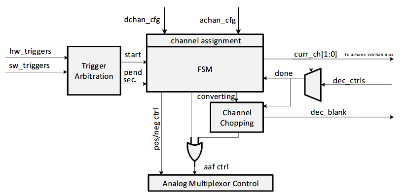
When triggered, the sequencer loads the input pin selection of the first assigned digital channel (see Digital part) then starts the decimator which initializes the modulator (see Delta-sigma modulator) to start the conversion.
The modulator output data is transferred to the assigned digital channel.
There are two supported conversion modes: incremental (single sample) and continuous. When a conversion is finished, the sequencer is notified by the decimator.
On-die temperature sensor
On-die temperature measurements are made with an internal temperature sensor by measuring bipolar "base-emitter voltage" (VBE) at different current densities and calculating temperature.
External temperature sensor
The external temperature sensor uses a fixed resistor and a temperature-dependent resistor (generally a negative temperature coefficient thermistor) - the resistor and thermistor form a voltage divider whose output voltage is temperature dependent. When enabled, the External Temperature Sensor block provides power to the off-chip temperature-dependent divider (and a reference supply for the ADC) of VDDD/3.
The AGC can automatically control the gain of either channel. AGC circuits typically monitor either the input voltage or output of the PGA and increase gain when signal amplitude is below a certain threshold or reduce gain when above another threshold. This function can also be achieved with a low-resolution A/D converter with digital comparison for gain selection.
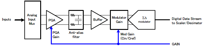
The analog portion of the ADCs consists:
The analog DSM system receives a differential signal selected through the analog multiplexer. This differential signal is received by a programmable gain amplifier (PGA). The output of the PGA feeds a low-pass anti-alias filter (AAF) with a bandwidth of ~30 kHz. A buffer amplifier drives the DSM modulator - this amplifier has high bandwidth to settle the modulator capacitors to better than 16 bits each time they are settled. The modulator uses capacitor dividers to set gain. The modulator is a third order with switched capacitor amplifier circuits. The modulator produces a multi-level digital bitstream sent to the digital channel. PGA and buffer amplifiers have offset trim, which reduces to offset these sub-blocks to <0.5 mV (across temperature). Offset trim is done during production. To reduce offset further, there is circuit chopping in PGA, buffer, and modulator. Chopping frequency is programmable from Fs/2 to Fs/256 (in 2's powers), where default is Fs/32. Fs here is the modulator clock.
Programmable gain amplifier (PGA)
The PGA is a fully-differential pseudo-instrumentation amplifier implemented with two Opamps. The PGA can be programmed for gains of 1 to 32. The PGA gain can be programmed via the internal bus or comes from the AGC. The PGA input range is -250 mV to 1.2 V (For RSH/RSL input pins, the input range is -300 mV to +300 mV). A negative pump is used to allow inputs to be below ground. This PGA has low-noise and input capacitance of about 1.5 pF. The PGA includes input/output chopping, which the sequencer can enable, and digital offset trim.
The anti-alias filter (AAF) is a first order RC filter with a 30-kHz corner frequency. 30 kHz is selected to give 40 dB attenuation at modulator sampling frequency, which is 3.072 MHz. The filter also has bypass switches, which allow the filter to be removed from the signal path, and a set of fast switches that bypass the "R" in the RC filter, moving the corner frequency approximately 600 kHz.
Following shows the AAF.
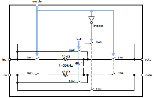
To alternately measure two signals with one channel, the anti-alias filter can be temporarily shorted since the AAF needs about 60 mks to settle to 16-bits before conversions can start - the measurement sample rate needs to slow to 4 ksps if the AAF is not bypassed.
The buffer amplifier converts the high-impedance AAF filter output to low impedance for driving the DSM modulator. The buffer includes digital offset trim and chopping, which can be enabled or disabled with a control signal.
The delta-sigma modulator works by taking the difference between input and feedback signals (delta) and accumulating that difference (sigma) to produce a digital output.
The digital stream goes to a decimator (see dchan), which converts the fast oversampled bit stream into slower high-resolution results.
The overcurrent detector (OCD) provides a safety mechanism to detect battery over current conditions. OCD detection is from the differential current sense inputs, RSHx and RSLx and support both charging and discharging over current. The detect threshold is programmable via an internal DAC. For safety, the OCD operated independently of the ADC which also provides faster detection of over current conditions. One OCD is associated with each set of current sense inputs (RSHx/RSLx).
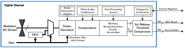
The digital data system has four digital channels that include:
The digital channels process outputs from either of the two analog channels. Two digital channels are with FIR filter and the others are without the FIR Filter. The digital channel without FIR filter has every other feature. The channels are typically used for current, voltage, temperature, and diagnostic measurements although they can be associated with any inputs. The digital system of the PACSS is largely autonomous; it performs acquisitions, filtering, post-processing, and data storage without firmware intervention. This allows real-time measurements without loading the CPU.
The digital data system optionally generates various interrupts to enable further processing of the results, or to handle diagnosis errors.
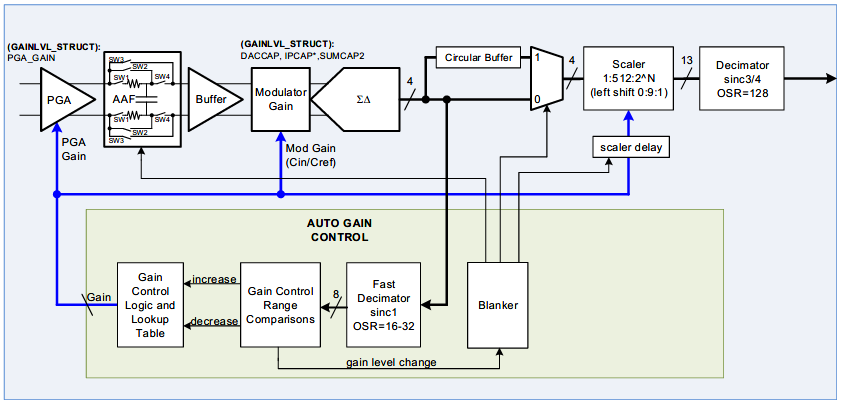
A scaler is used so the LSB of the ADC can have the same weight regardless of gain. The LSB is established by the ADC resolution at maximum gain - for the current channel, the LSB is 0.715 mA with a gain of 512. The scaler multiplies the output of the modulator by 512/Gain to normalize results and maintain 0.715 mA for the LSB regardless of gain setting. To multiply by 2, the scaler shifts results up one bit. To cover a gain range of 1 to 512 means results can be shifted up to 9 bits.
There are two decimators - one is configurable as Sinc3 or Sinc4, and the other is used as rate reducer and is a Sinc2. The first decimator can be configured for third or fourth order operation. The decimation rate (DR) is programmable and can range from 2 to 128. Both the third and fourth order decimator configurations can be used for incremental or continuous mode.
The second decimator (rate reducer) DR2 is programmable and can range from 1 to 32.
Compensation block multiplies results for gain adjustment and adds constants for offset correction. Up to 64 tap finite impulse response (FIR) filter with programmable coefficients follows the compensation block. Results are then normalized to remove unused bits and averaging, accumulation, and threshold detection can be performed.
This section describes the process of initializing the on-die temperature sensor using the Delta-Sigma ADC (DSADC). The initialization includes enabling the temperature sensor, configuring the measurement parameters, performing the measurements to calculate the current ratio for calibration and then performing the temperature measurements.
This snippet demonstrates how to create and initialize the configuration structures for the on-die temperature sensor.
Two configurations are defined:
Initialization and Calibration
To ensure proper initialization during configuration, it is important to maintain appropriate delays. Temperature measurement occurs in two stages: first, on-die calibration is performed, and only after that, the actual temperature measurement is conducted.
After enabling the on-die sensor, the structures are initialized using the Cy_DSADC_InitializeDieTempConfigs function to perform two current measurements on the resistor for 1x and 9x currents. The obtained values are shifted as required for 29-bit measurements and passed to the Cy_DSADC_CalcCurrentRatio function to get the ratio of the resistor measurements and normalize the results.
The temperature measurement process requires reconfiguring the on-die structures to measure the temperature using the transistor load mode CY_DSADC_TEMPERATURE_MEASUREMENT_TRANSISTOR. Result of two measurements are shifted as required for 29-bit measurements and calculated before value currentRatio passed to the function Cy_DSADC_CalcDieTemp to calculate the temperature in fixed point Q12.20 format.
| Version | Changes | Reason for Change |
|---|---|---|
| 1.10 | The OCD feature support was added for PSOC4 HVPA SPM 1.0 device. | New feature support. |
| Updated interfaces of Cy_DSADC_CountsTo_Volts, Cy_DSADC_CountsTo_mVolts, Cy_DSADC_CountsTo_uVolts. | Defect fix | |
| 1.0 | Initial version |