MTB CAT1 Peripheral driver library
All Data Structures Functions Variables Typedefs Enumerations Enumerator Modules Pages


To start the procedure, perform Configuration Example and Initialization with included extra channel, which can be re-used after this procedure is complete:

/* Scenario: Third channel was selected to be used in the calibration
* procedure. */
cy_stc_sar2_channel_config_t pass_0_saradc_0_sar_0_channel_2_config =
{
.channelHwEnable = true,
.triggerSelection = CY_SAR2_TRIGGER_OFF,
.channelPriority = 0U,
.isGroupEnd = true,
.pinAddress = 0U,
.portAddress = 0U,
.extMuxEnable = false,
.extMuxSelect = 0U,
.preconditionMode = CY_SAR2_PRECONDITION_MODE_OFF,
.overlapDiagMode = CY_SAR2_OVERLAP_DIAG_MODE_OFF,
.sampleTime = 120U,
.postProcessingMode = CY_SAR2_POST_PROCESSING_MODE_NONE,
.resultAlignment = CY_SAR2_RESULT_ALIGNMENT_RIGHT,
.averageCount = 1U,
.rightShift = 0U,
.positiveReload = 0U,
.negativeReload = 0U,
.rangeDetectionLoThreshold = 0U,
.rangeDetectionHiThreshold = 4095U,
};

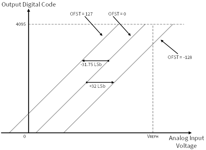
The ADC has an offset adjustment function to compensate for offset error.

It is possible to select code from +127 to -128 in a dec. for analog calibration.
The offset adjustment step is a quarter of 1LSb.
Offset = max( 0, min( 4095, floor( VIN/VREFH x 4096 + OFST/4 ) ) )

sar2_offset_calibration.png
Note
Enable reference buffer mode using Cy_SAR2_SetReferenceBufferMode function.


Following code snippet can be used:

/* Scenario: SAR2 block 0 with it's clock source is configured, channel 2 is
* not used. */
/* Calibration initial setting. */
{
.offset = 127ul,/* Offset Calibration start setting */
.gain = 15ul,/* Gain Calibration start setting */
};
/*******************************************************************************
* Function Name: getAdcValue
********************************************************************************
*
* Issues software trigger for the channel 2, waits for SAR2 block to complete
* it's calculation and returns calculated value.
*
* \return
* Measurement value
*
*******************************************************************************/
uint16_t getAdcValue(void)
{
/* Trigger ADC. */
/* Wait for group of single channel to complete. */
/* Get the result(s) */
return (Cy_SAR2_Channel_GetResult(PASS0_SAR0, 2U, NULL));
}
/*******************************************************************************
* Function Name: offset_Calibration
********************************************************************************
*
* Performs SAR block offset calibration
*
* \return
* Boolean value if calibration was successful.
*
*******************************************************************************/
bool offset_Calibration(void)
{
/* Start ADC conversion and get the ADC value */
int16_t result = getAdcValue();
int16_t offset_VREFH = 0U;
int16_t offset_VREFL = 0U;
uint32_t value = 0U;
pass_0_saradc_0_sar_0_channel_2_config.pinAddress = CY_SAR2_PIN_ADDRESS_VREF_L;
Cy_SAR2_SetAnalogCalibrationValue(PASS0_SAR0, &calibrationConfig);
/* Initialize channel. */
Cy_SAR2_Channel_Init(PASS0_SAR0, 2U, &pass_0_saradc_0_sar_0_channel_2_config);
if(result > 0)
{
/* Decrement the Value of Offset Compensation by "1" */
for(offset_VREFL = 127; offset_VREFL >= -128; offset_VREFL -= 1)
{
/* Set "offset_VREFL" to offset register value */
calibrationConfig.offset = offset_VREFL;
Cy_SAR2_SetAnalogCalibrationValue(PASS0_SAR0, &calibrationConfig);
/* Get ADC conversion value. */
result = getAdcValue();
/* Does the ADC conversion value equal to 0? */
if(result == 0)
{
break;
}
/* If offset has reached lower bound. */
if(offset_VREFL == -128)
{
/* Report error. */
return false;
}
}
}
else
{
/* End of Offset Adjustment with Abnormality. */
return false;
}
/* Set VREFH Voltage to Input */
pass_0_saradc_0_sar_0_channel_2_config.pinAddress = CY_SAR2_PIN_ADDRESS_VREF_H;
/* Set Offset Compensation to "-128" and init channel. */
calibrationConfig.offset = -128;
Cy_SAR2_SetAnalogCalibrationValue(PASS0_SAR0, &calibrationConfig);
Cy_SAR2_Channel_Init(PASS0_SAR0, 2u, &pass_0_saradc_0_sar_0_channel_2_config);
/* Start ADC Conversion and get the A/D value. */
result = getAdcValue();
/* Is the ADC Conversion value lower than 0xFFF */
if(result < 0xFFF)
{
/* Increment the Value of Offset Compensation by "1". */
for(offset_VREFH = -128; offset_VREFH <= 127; offset_VREFH += 1)
{
/* Set "offset_VREFH" to offset register value. */
calibrationConfig.offset = offset_VREFH;
Cy_SAR2_SetAnalogCalibrationValue(PASS0_SAR0, &calibrationConfig);
/* Get ADC Conversion value. */
result = getAdcValue();
/* Does the ADC Conversion value Equal to "4095"? */
if(result == 0xFFF)
{
break;
}
/* Does the value of offset compensation equal to "127"? */
if(offset_VREFH == 127)
{
/* Offset adjustment failed - report error. */
return false;
}
}
}
else
{
/* Offset adjustment failed - report error. */
return false;
}
/* Does "(floor((offset_VREFH+offset_VREFL)/2) + 2)" greater than "125" ?*/
value = (floor((offset_VREFH+offset_VREFL)/2U) + 2U);
if(value > 125U)
{
/* Offset adjustment failed - report error. */
return false;
}
/* Set the value of offset compensation to (floor((offset_VREFH+offset_VREFL)/2) + 2) */
calibrationConfig.offset = (floor((offset_VREFH+offset_VREFL)/2U) + 2U);
return true;
}

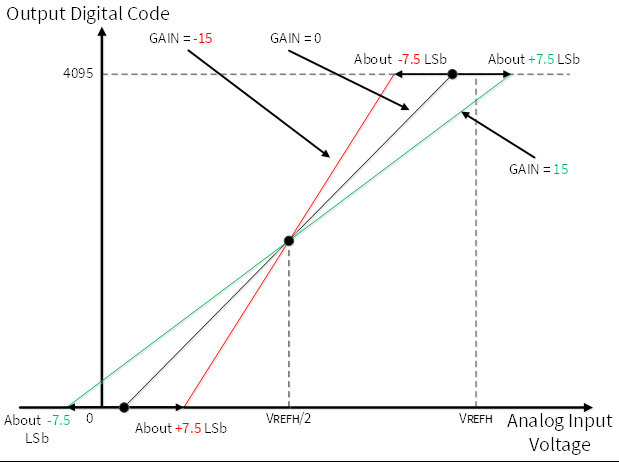
After that, the Gain should also be calibrated as well. The ADC has a gain adjustment function to compensate for gain error. It is possible to set code from +15 to -15 dec. The gain adjustment step is a quarter of 1LSb.
Gain = max(0, min(4095, floor((4096 - GAIN)/VREFH x (VIN - VREFH/2) + 2048)))

sar2_gain_calibration.png
/* Scenario: SAR2 block 0 is left after offset calibration intact, global
* structure is still available with offset calibration results. */
/*******************************************************************************
* Function Name: gain_Calibration
********************************************************************************
*
* Performs SAR block gain calibration
*
* \return
* Boolean value if calibration was successful.
*
*******************************************************************************/
bool gain_Calibration(void)
{
int16_t gain;
int16_t result = 0U;
/* Set Gain Correction setting to "15". */
calibrationConfig.gain = 15;
/* Set VREFL Voltage to Input and init the channel. */
pass_0_saradc_0_sar_0_channel_2_config.pinAddress = CY_SAR2_PIN_ADDRESS_VREF_L;
Cy_SAR2_Channel_Init(PASS0_SAR0, 2u, &pass_0_saradc_0_sar_0_channel_2_config);
/* Apply the initial calibration settings. */
Cy_SAR2_SetAnalogCalibrationValue(PASS0_SAR0, &calibrationConfig);
/* Start ADC value Conversion */
result = getAdcValue();
if(result > 0)
{
for(gain = 15; gain >=-14; gain -= 1)
{
/* Set gain to register */
calibrationConfig.gain = gain;
Cy_SAR2_SetAnalogCalibrationValue(PASS0_SAR0, &calibrationConfig);
result = getAdcValue();
if(result == 0)
{
/* Set gain compensation to "gain - 1" */
calibrationConfig.gain = gain - 1;
Cy_SAR2_SetAnalogCalibrationValue(PASS0_SAR0, &calibrationConfig);
break;
}
if(gain == -14)
{
/* Gain adjustment failed - report error. */
return false;
}
}
}
return true;
}


Once done, the calibrationConfig global structure contains calibration data for SAR2 block 0. Calibration is advised to be done as frequent as possible.