 |
MTB CAT1 Peripheral driver library
|
|
MTB CAT1 Peripheral driver library
|
Internal flash memory programming.
The functions and other declarations used in this driver are in cy_flash.h. You can include cy_pdl.h to get access to all functions and declarations in the PDL.
Flash memory in PSoC devices provides non-volatile storage for user firmware, user configuration data, and bulk data storage.
Flash operations are implemented as system calls. System calls are executed out of SROM in the privileged mode of operation. Users have no access to read or modify the SROM code. The driver API requests the system call by acquiring the Inter-processor communication (IPC) and writing the SROM function opcode and parameters to its input registers. As a result, an NMI interrupt is invoked and the requested SROM function is executed. The operation status is returned to the driver context and a release interrupt is triggered.
Writing to flash can take up to 20 milliseconds. During this time, the device should not be reset (including XRES pin, software reset, and watchdog) or unexpected changes may be made to portions of the flash. Also, the low-voltage detect circuits should be configured to generate an interrupt instead of a reset.
A Read while Write violation occurs when a flash Read operation is initiated in the same or neighboring (neighboring restriction is applicable just for the CY8C6xx6, CY8C6xx7 devices) flash sector where the flash Write, Erase, or Program operation is working. This violation may cause a HardFault exception. To avoid the Read while Write violation, carefully split the Read and Write operation on flash sectors which are not neighboring, considering both cores in the multi-processor device. If the flash is divided into four equal sectors, you may edit the linker script to place the code into neighboring sectors. For example, use sectors number 0 and 1 for code and sectors 2 and 3 for data storage.
The CAT1A devices user-programmable Flash consists of:
The CAT1C devices user-programmable Flash consists of:
Write operation may be done as Blocking or Partially Blocking, defined as follows:
In this case, the entire Flash block is not available for the duration of the Write (∼16ms). Therefore, no Flash accesses (from any Bus Master) can occur during that time. CPU execution can be performed from SRAM. All pre-fetching must be disabled. Code execution from Flash is blocked for the Flash Write duration for both cores.
This method has a much shorter time window during which Flash accesses are not allowed. Application code execution from Flash is blocked for only a part of Flash Write duration, for both cores. Blocking duration depends upon the API sequence used.
For CAT1A Devices API sequence Cy_Flash_StartEraseRow() + Cy_Flash_StartProgram() there are four block-out regions during which Read is blocked. See Figure 1.
For CAT1C devices Flash memory controller has the dual bank mode feature. When using dual bank mode, flash memory region is split into two half banks. One is called Logical Bank 0 and the other is called Logical Bank 1 User will be able to read from a different logical bank while writing to one logical bank.
For CAT1C devices Erase ROW is not supported. User has to erase the entire sector before writing to the sector.
CM7 cores in CAT1C devices support Data Cache. Data Cache line is 32 bytes. User needs to make sure that the pointer passed to the following functions points to 32 byte aligned data. Cy_Flash_StartWrite, Cy_Flash_ProgramRow, Cy_Flash_Program and Cy_Flash_Program_WorkFlash. User can use CY_ALIGN(32) macro for 32 byte alignment.
CAT1B devices run on single core and hence IPC is not used for erase and write operations on flash memory.
| Block-out | Phase | Duration |
|---|---|---|
| A | The beginning of the Erase operation | 2ms + 9500 SlowClk cycles |
| B | The end of the Erase operation | 0.13ms + 1000 SlowClk cycles |
| C | The beginning of the Program operation | 0.8ms + 6000 SlowClk cycles |
| D | The end of the Program operation | 0.13ms + 1000 SlowClk cycles |
This allows both cores to execute for about 80% of Flash Write operation - see Figure 1. This capability is important for communication protocols that rely on fast response.
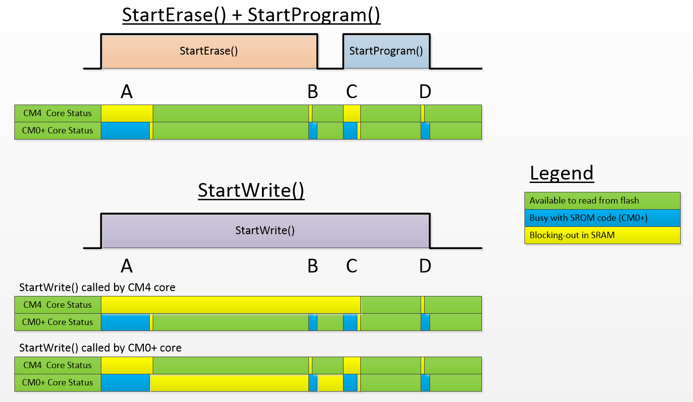
For the Cy_Flash_StartWrite() function, the block-out period is different for the two cores. The core that initiates Cy_Flash_StartWrite() is blocked for two periods:
The core that performs read/execute is blocked identically to the previous scenario - see Figure 1.
This allows the core that initiates Cy_Flash_StartWrite() to execute for about 20% of Flash Write operation. The other core executes for about 80% of Flash Write operation.
In CAT1B devices with flash IP CY_IP_MXS40FLASHC When refresh is enabled, for each row an extra 16 bytes is used for storing refresh related data. User need to make sure that this data is not corrupted while writing and erasing the row data. When refresh is enabled row size has to be considered as CY_FLASH_SIZEOF_ROW + 16Bytes
Some constraints must be planned for in the Partially Blocking mode which are described in detail below.
Writing rules in application flash (this restriction is applicable just for CY8C6xx6, CY8C6xx7 devices):
Suggestion: in case of bootloading, it is recommended to place code for CM4 in either S0 or S1. CM0+ code resides in S0. Write data to S2 and S3 sections.
If you plan to use "cy_em_eeprom" section for different purposes for both of device cores or use Em_EEPROM Middleware together with flash driver write operations you must modify the linker scripts.
For more information, refer to the Middleware/Infineon Em_EEPROM Middleware Library section of the PDL documentation.
See the technical reference manual (TRM) for more information about the Flash architecture.
| Version | Changes | Reason for Change |
|---|---|---|
| 3.150.1 | Updated driver documentation text. | Documentation update. |
| 3.150 | Extend api with base pointer to support devices with multiple FLASHC instances. | Code enhancement. |
| 3.140 | Fixed the compatibility issues encountered when building projects in EWARM using the "C++ only" option. | Bug fixes |
| Callback API's for PSOC control devices. | Code enhancement. | |
| 3.130 | Updated status code for Cy_Flash_Refresh and Cy_Flash_Init. Updated cy_en_flashdrv_status_t with new status codes. | Code enhancement. |
| 3.120 | Updated internal implementation for PSOC C3 device. | Code enhancement. |
| 3.110 | In Cy_Flash_SendCmd, waiting for CM0 to be ready to accept command. | |
| 3.100 | Added support for PSOC C3 (CAT1B). Added flash refresh feature. Added inject ecc disable and corrected address in inject ecc. | Added support for new devices, added new feature and code enhancement. |
| 3.90 | Added support for TRAVEO™ II Body Entry devices. Updated pre-processor check to only include code if ECT flash is not used. In cy_flash_srom, changed pre-processor checks from using CM7 availability to using MXFLASHC ver. to determine flash hardware availability. In cy_flash_srom, added interrupt compatibility for CM4 devices. | Code enhancement and support for new devices. |
| 3.80 | Dual bank support added for CAT1A devices. | Newly added APIs Cy_Flashc_SetMain_Flash_Mapping , Cy_Flashc_SetWork_Flash_Mapping for CAT1A and CAT1C devices. |
| 3.70 | Fixed MISRA 2012 violations and Documentation Update. | MISRA 2012 compliance. |
| 3.60 | Added API's to support new product family. Enhancement for support of eCT flash. | eCT flash's contains Code flash and Work flash. New API's to program/erase both work flash and code flash are added. |
| 3.50.1 | Updated documentation to limit devices with the restrictions. | User experience enhancement. |
| 3.50 | Updated attribute usage for the linker section placement. | Enhancement based on usability feedback. |
| Fixed/documented MISRA 2012 violations. | MISRA 2012 compliance. | |
| 3.40 | Updated Cy_Flash_OperationStatus() to access protected registers. | Added PSoC 64 device support. |
| 3.30.4 | Improved documentation. | User experience enhancement. |
| 3.30.3 | Updated documentation to limit devices with the restrictions. Improved calculation of the CY_FLASH_DELAY_CORRECTIVE macro. | User experience enhancement. |
| 3.30.2 | Updated documentation to limit devices with the neighboring restriction. | User experience enhancement. |
| 3.30.1 | Used the CY_RAMFUNC_BEGIN and CY_RAMFUNC_END macros that allocate the function in RAM instead of using the CY_SECTION(".cy_ramfunc") macros. | Removed the code duplication. |
| 3.30 | Moved ipcWaitMessageStc structure to the RAM section called ".cy_sharedmem". | Support Secure Boot devices. |
| Renamed Function Cy_Flash_StartErase() to Cy_Flash_StartEraseRow(). | The driver improvements based on the usability feedback. | |
| Added new API functions Cy_Flash_EraseSector, Cy_Flash_StartEraseSector, Cy_Flash_EraseSubsector, Cy_Flash_StartEraseSubsector | The driver improvements based on the usability feedback. | |
| 3.20 | Flattened the organization of the driver source code into the single source directory and the single include directory. | Driver library directory-structure simplification. |
| Added new API function Cy_Flash_InitExt | The driver improvements based on the usability feedback | |
| Added register access layer. Use register access macros instead of direct register access using dereferenced pointers. | Makes register access device-independent, so that the PDL does not need to be recompiled for each supported part number. | |
| 3.11 | Updated driver functionality to correctly use the SysClk measurement counters while partially blocking flash operations | Added arbiter mechanism for correct usage of the SysClk measurement counters |
| 3.10 | Updated Cy_Flash_SendCmd() code to support single core devices. | Support new devices |
| 3.0 | New function - Cy_Flash_ProgramRow(); Updated Cy_Flash_RowChecksum(): changed input parameter to take the row address (rowAddr) instead of the row number (rowNum); Renamed macro for disabling RWW support in driver to CY_FLASH_RWW_DRV_SUPPORT_DISABLED. Updated Configuration Considerations documentation section with flash usage constraints. | Improvements made based on usability feedback to use a common interface |
| 2.0 | Added non-blocking erase function - Cy_Flash_StartErase(). Removed the clear cache function call. | The clear cache operation is removed from the blocking Write/Erase function because in this case it is performed by the hardware. Otherwise it is documented that it is the user's responsibility to clear the cache after executing the non-blocking Write/Erase flash operation. |
| Added new Cy_Flash_IsOperationComplete() function to check completeness. Obsoleted Cy_Flash_IsWriteComplete(), Cy_Flash_IsProgramComplete(), and Cy_Flash_IsEraseComplete() functions. Added Cy_Flash_GetExternalStatus() function to get unparsed status where flash driver will be used in security applications with other modules as SecureImage. Added Cy_Flash_Init() function to initialize all needed prerequisites for Erase/Write operations. | Updated driver design to improve user experience. | |
| Updated driver implementation to remove MISRA rules deviations. | Driver implementation quality improvement. | |
| 1.0 | Initial version |
API Reference | |
| Macros | |
| Functions | |
| Enumerated Types | |
| Structures | |